Silicon wafer cleaner and silicon wafer cleaning method

A silicon wafer cleaning and silicon wafer technology, which is applied in cleaning methods and utensils, cleaning methods using liquids, chemical instruments and methods, etc. The effect of production efficiency

Active Publication Date: 2011-09-28
SHANGHAI HUAHONG GRACE SEMICON MFG CORP
View PDF0 Cites 2 Cited by
  • Summary
  • Abstract
  • Description
  • Claims
  • Application Information

AI Technical Summary

Problems solved by technology

At present, ultrasonic cleaning tanks are generally used to clean silicon wafers, but the commonly used ultrasonic cleaning tanks can only clean a whole batch of silicon wafers, and cannot clean a single silicon wafer

Method used


Image

  • Silicon wafer cleaner and silicon wafer cleaning method
  • Silicon wafer cleaner and silicon wafer cleaning method
  • Silicon wafer cleaner and silicon wafer cleaning method

Examples


Embodiment Construction

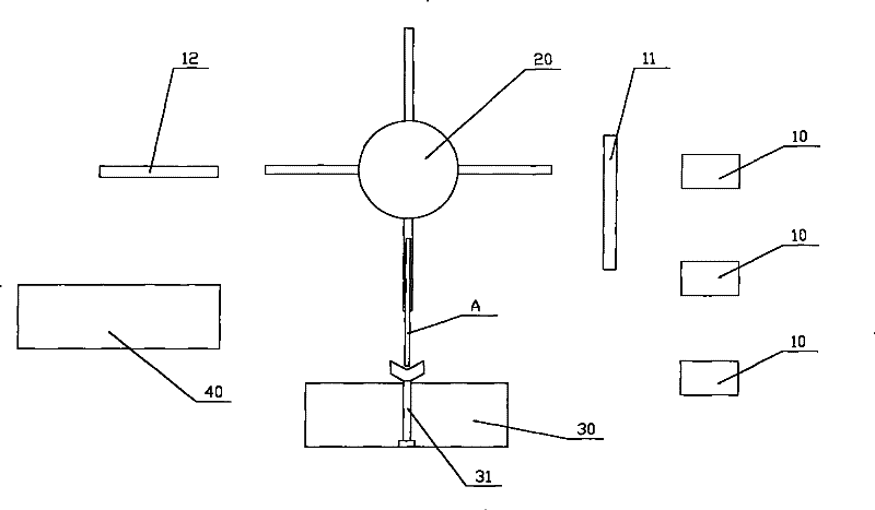
[0038] Such as figure 1 As shown, the silicon wafer cleaning machine of the present invention includes a silicon wafer carrying table 10 , a rotating arm 20 , a silicon wafer cleaning tank 30 , and a spin drying unit 40 .

[0039] One side of the rotating arm 20 is provided with a silicon wafer carrier 10, and the silicon wafer carrier 10 is used to place silicon wafers to be cleaned; a silicon wafer cleaning tank 30 is arranged below the rotating arm 20, and the silicon wafer cleaning tank 30 is used for cleaning and immersing in the tank silicon wafers; the other side of the rotating arm 20 is provided with a spin drying unit 40, which is used to dry the cleaned silicon wafers.

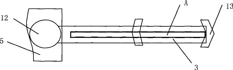
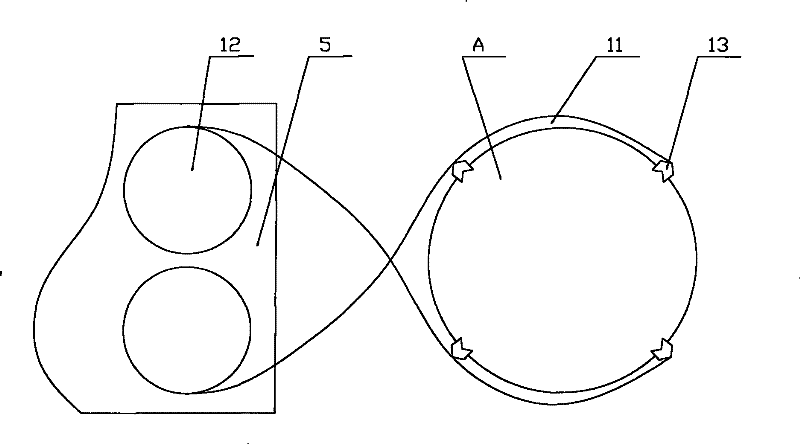
[0040] A transfer rod 11 is arranged between the rotating arm 20 and the silicon wafer carrier 10, and the transfer rod 11 is used to extract silicon wafers from the silicon wafer carrier 10 and transfer them to the rotating arm 20; There is a transfer rod 12 for transferring the silicon wafers on ...


PUM


Abstract

The invention discloses a silicon wafer cleaner which comprises a silicon wafer bearing stand, a rotating arm, a silicon wafer cleaning tank and a rotating drying unit, wherein the silicon wafer bearing stand is arranged at one side of the rotating arm; the silicon wafer cleaning tank is arranged below the rotating arm; a silicon wafer receiver is arranged in the silicon wafer cleaning tank; the rotating drying unit is arranged at one side or the other side of the rotating arm; and transferring rods are arranged between the rotating arm and the silicon wafer bearing stand and between the rotating arm and the rotating drying unit. In the invention, a full automatic silicon wafer transferring mode is adopted to continuously and automatically treat a single silicon wafer, and can meet the requirements of the increasingly complicated production processes. As the equipment can carry out automatic cleaning, manual cleaning is not needed, thus preventing the risk of contaminating and scratching the silicon wafers and the like caused by manual cleaning, and simultaneously improving production efficiency. The invention also discloses a method for cleaning the silicon wafers by the silicon wafer cleaner.

Description

technical field [0001] The invention relates to semiconductor manufacturing equipment, in particular to a silicon wafer cleaning machine, and also relates to a silicon wafer cleaning method. Background technique [0002] During the manufacture of integrated circuits, silicon wafers need to be cleaned. At present, ultrasonic cleaning tanks are generally used to clean silicon wafers, but the commonly used ultrasonic cleaning tanks can only clean a whole batch of silicon wafers, and cannot clean a single silicon wafer. Contents of the invention [0003] The technical problem to be solved by the present invention is to provide a silicon wafer cleaning machine, which can continuously process a single silicon wafer. [0004] For solving the problems of the technologies described above, the technical solution of the silicon wafer cleaning machine of the present invention is: [0005] It includes a silicon wafer carrying table, a rotating arm, a silicon wafer cleaning tank, and ...

Claims


Application Information

Patent Timeline
Patent Type & Authority Patents(China)
IPC IPC(8): H01L21/00H01L21/02H01L21/306H01L21/677B08B3/12
Inventor 宁开明
Owner SHANGHAI HUAHONG GRACE SEMICON MFG CORP
Why Eureka
Try Eureka