Joint surface detecting structure and joint surface detecting method

A technology for detecting structures and methods, applied in the direction of measuring electricity, measuring devices, measuring electrical variables, etc., can solve the problem that the flip-chip manufacturing process does not meet the manufacturing process specifications, the flip-chip manufacturing process does not meet the specifications, and the manufacturing process precision connection bumps Pressing deformation does not meet the manufacturing process specifications and other issues

Inactive Publication Date: 2010-02-24
AU OPTRONICS CORP
View PDF0 Cites 1 Cited by
  • Summary
  • Abstract
  • Description
  • Claims
  • Application Information

AI Technical Summary

Problems solved by technology

However, please refer to Figure 1B As shown, when the bonding bump 12 covers any of the alignment marks 11a-11d, it means that the flip-chip manufacturing process does not meet the specifications.
[0004] From the above, it can be seen that the current technology can only judge that the flip-chip manufacturing process does not meet the manufacturing process specifications, but it is impossible to know whether the reason is due to the accuracy of the manufacturing process, the tolerance of the incoming material of the connecting bump itself, or the excessive deformation of the pressing Non-compliance with manufacturing process specifications caused by factors such as

Method used


Image

  • Joint surface detecting structure and joint surface detecting method
  • Joint surface detecting structure and joint surface detecting method
  • Joint surface detecting structure and joint surface detecting method

Examples


Embodiment Construction

[0048] A joint surface detection structure and a joint surface detection method according to preferred embodiments of the present invention will be described below with reference to related drawings, wherein the same elements will be described with the same reference symbols.

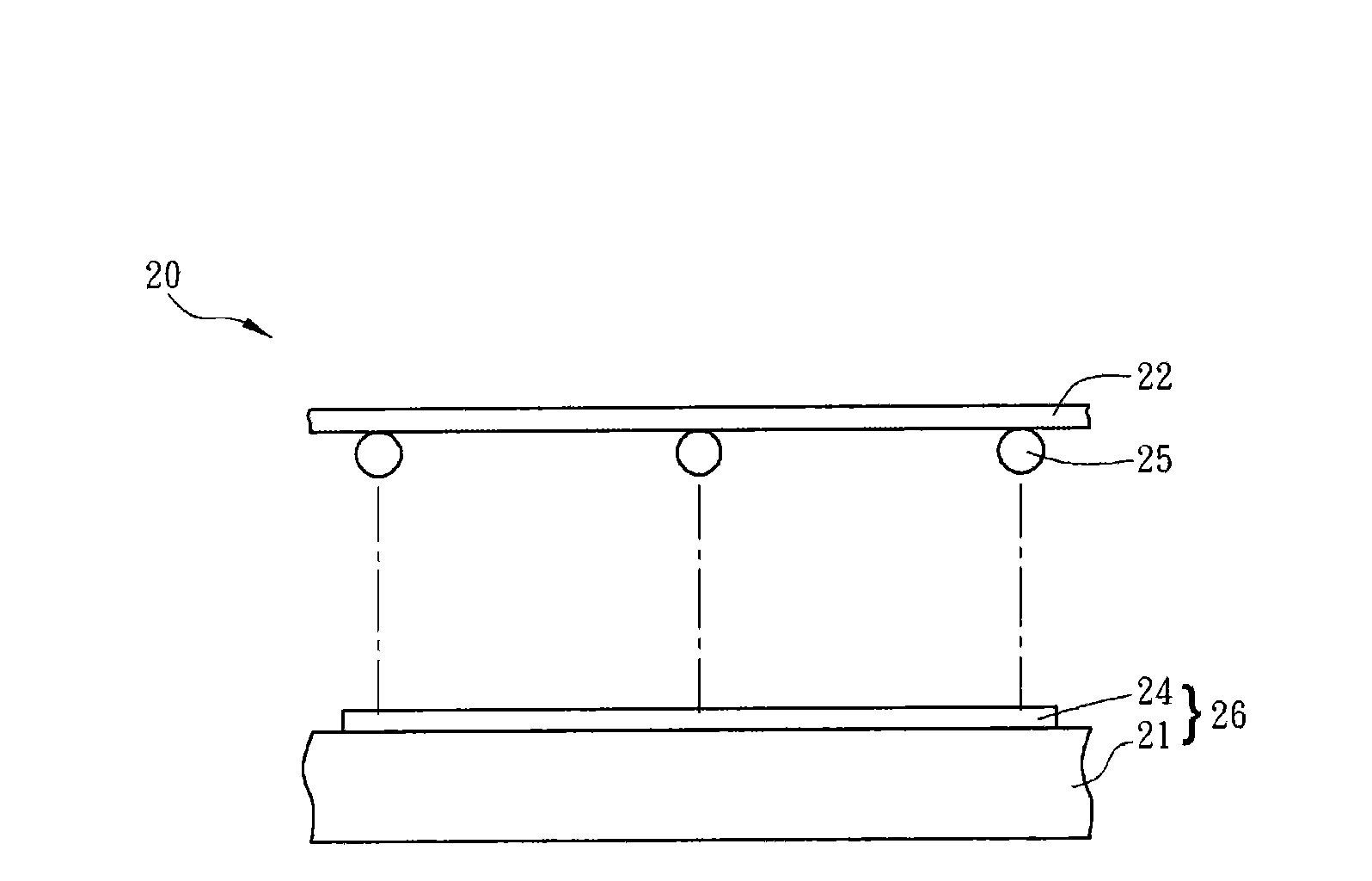
[0049] figure 2 It is a schematic side view of a chip on glass (COG) structure of the present invention. Please refer to figure 2 As shown, the chip-on-glass structure 20 includes a chip 22 and a glass substrate 21 . The chip 22 is mainly intended to be electrically connected to an electrical connection pad (pad) of a circuit on the glass substrate 21. In this embodiment, a plurality of connection bumps 25 are arranged between the chip 22 and the glass substrate 21, which can be pre-installed. The electrical connection pads disposed on the glass substrate 21 may be pre-disposed on a surface of the chip 22 , wherein the connection bumps 25 are, for example, solder balls or gold bumps.

[0050] In or...


PUM


Abstract

The invention provides a joint surface detecting structure and a joint surface detecting method. The joint surface detecting structure comprises a glass substrate and a judging pattern, wherein the judging pattern is arranged on one surface of the glass substrate, and comprises a metal marker, a minimum joint judging area and a virtual detecting marker. The metal marker is provided with a closed area, the minimum joint judging area is positioned in the closed area of the metal marker, the virtual detecting marker is arranged between an outer edge and an inner edge of the metal marker. Throughthe relationship between the judging pattern and the virtual detecting marker, the invention can judge the problems of precision of manufacturing process, allowance of materials of connecting lugs oroverlarge lamination deformation which result in not conforming to the standard.

Description

technical field [0001] The invention relates to a joint surface detection structure and a joint surface detection method, in particular to a joint surface detection structure and a joint surface detection method for glass-on-chip substrates. Background technique [0002] In the current common chip-on-glass (COG) manufacturing process, a chip is connected to a connection pad on a glass substrate through connection bumps such as solder balls or gold bumps. (pad) bonding, and the bonding method generally uses a pressure bonding method to connect the connecting bumps to the chip and the glass substrate. However, since the dimensions of the connecting bumps have tolerances, and the connecting bumps will be deformed due to force during the pressing process, there is inconsistency in the size of the connecting bumps after pressing, so that it is impossible to accurately know the relationship between the connecting bumps and the connecting bumps. Whether the bonding surface area of...

Claims


Application Information

Patent Timeline
Patent Type & Authority Applications(China)
IPC IPC(8): G01R31/02
Inventor 黄柏辅石崇甫林世雄
Owner AU OPTRONICS CORP
Why Eureka
Try Eureka