Eureka AIR delivers breakthrough ideas for toughest innovation challenges, trusted by R&D personnel around the world.

Nonvolatile memory and manufacturing method thereof

A non-volatile, manufacturing method technology, applied in semiconductor/solid-state device manufacturing, electric solid-state devices, semiconductor devices, etc., can solve problems such as disadvantages of portable electronic products, and achieve the effect of improving coupling rate and component performance.

Active Publication Date: 2009-12-02
HEJIAN TECH SUZHOU
View PDF0 Cites 7 Cited by
  • Summary
  • Abstract
  • Description
  • Claims
  • Application Information

AI Technical Summary

Problems solved by technology

The above situation is quite unfavorable for the application of memory components in the field of portable electronic products with low energy consumption requirements

Method used


Image

  • Nonvolatile memory and manufacturing method thereof
  • Nonvolatile memory and manufacturing method thereof
  • Nonvolatile memory and manufacturing method thereof

Examples


Embodiment Construction

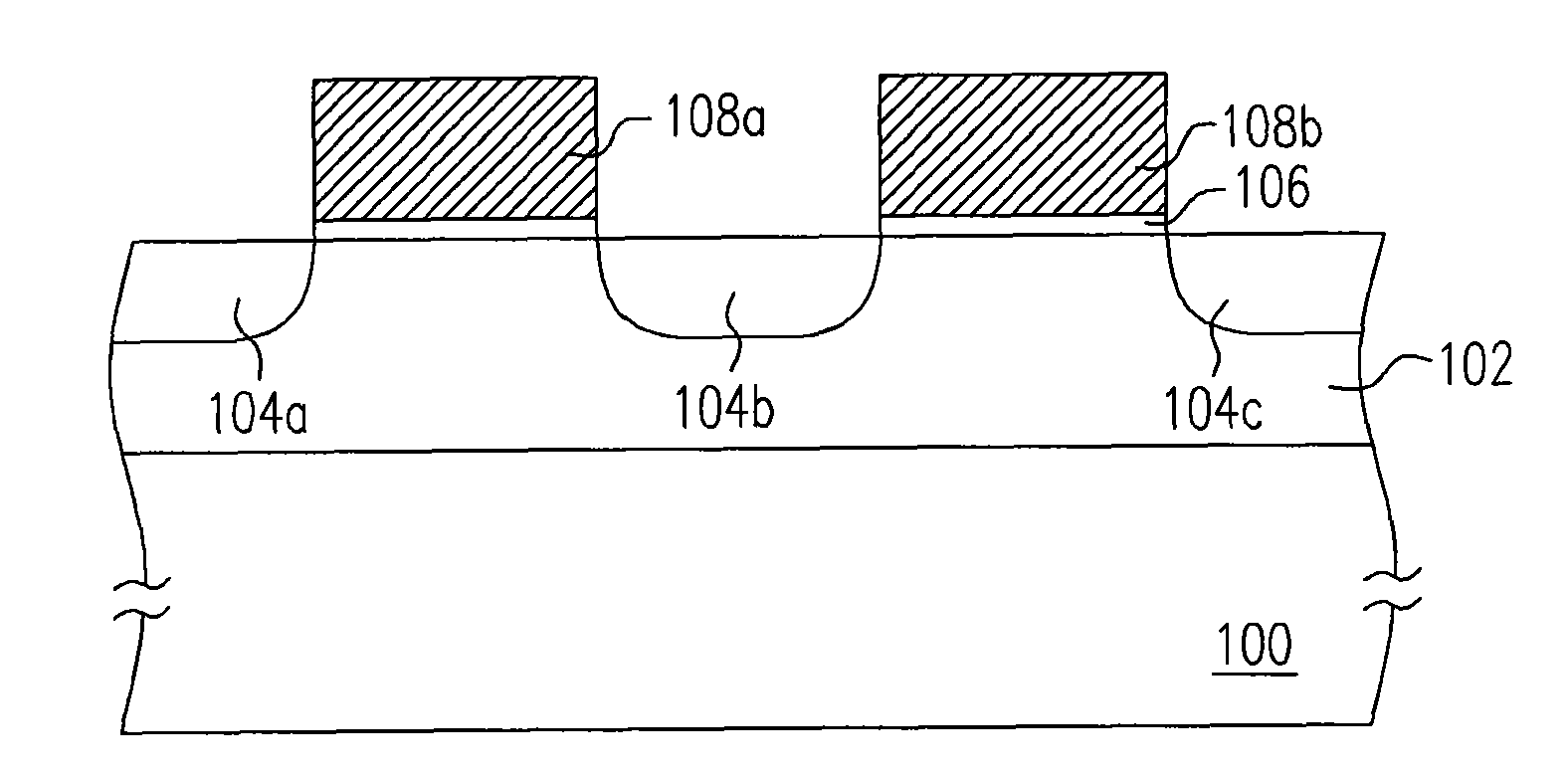
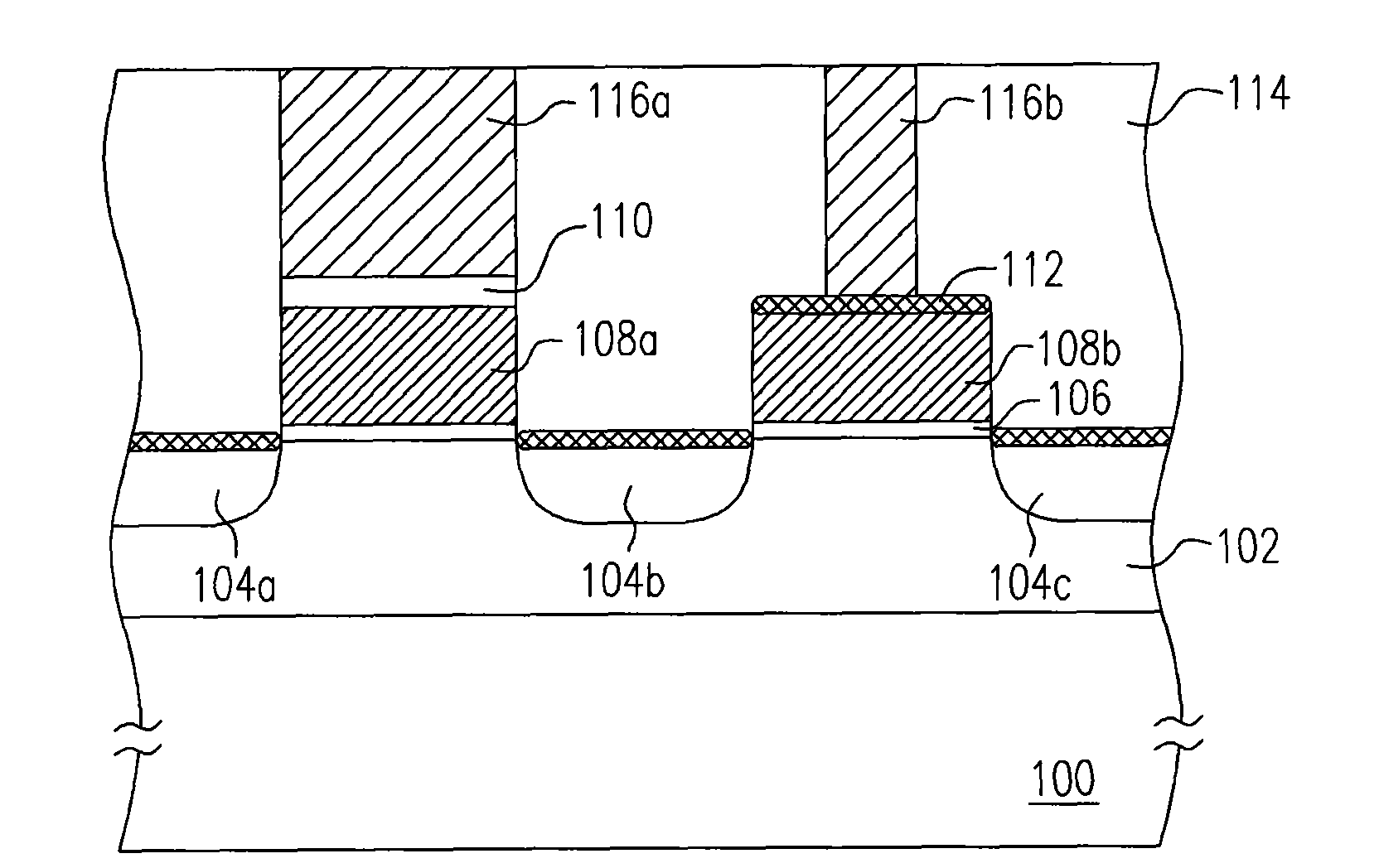
[0035] Figure 1A to Figure 1D is a schematic cross-sectional view of the manufacturing process of the non-volatile memory according to an embodiment of the present invention. It should be noted that the manufacturing method of the non-volatile memory described below is only one of various types of non-volatile memory, that is to say, the following embodiment is to form a one-time programmable read-only The structure of the memory is described as an example, which is mainly to enable those skilled in the art to implement it, but is not intended to limit the scope of the present invention. As for the configuration, formation method and formation sequence of other components such as gates, doped regions, metal silicides, etc., they can be fabricated according to techniques known to those skilled in the art, and are not limited to the following examples. .

[0036] Please refer to Figure 1A , providing a substrate 100 . The substrate 100 is, for example, a semiconductor subst...


PUM


Abstract

The invention discloses a nonvolatile memory which comprises a substrate, a plurality of doped regions, a first grid, a conductor layer, a first contact window plug and a dielectric layer, wherein the doped regions are arranged in the substrate; the first grid is arranged on the substrate between two adjacent doped regions; the conductor layer is arranged above the first grid; the first contact window plug is arranged between the first grid and the conductor layer; and the dielectric layer is arranged between the first grid and the first contact window plug.

Description

technical field [0001] The present invention relates to a semiconductor component and its manufacturing method, and in particular to a non-volatile memory and its manufacturing method. Background technique [0002] Non-volatile memory components have become popular in personal computers and electronic devices due to their characteristics of repeatable data storage, reading and erasing, and the advantage that the stored data can still be stored after power failure. A widely used memory component. Non-volatile memory can be subdivided into programmable read-only memory (programmable read-only memory, PROM), erasable programmable read-only memory (erasable programmable ROM, EPROM), electronic erasable programmable read-only memory ( Electrically erasable programmable ROM, EEPROM), mask read-only memory (mask ROM), one-time programmable read-only memory (one-time programmable read-only memory, OTPROM), etc. [0003] Generally speaking, the coupling ratio of the gate is one of ...

Claims


Application Information

Patent Timeline
Patent Type & Authority Applications(China)
IPC IPC(8): H01L27/112H01L27/115H01L23/522H01L21/8246H01L21/8247H01L21/768H10B20/00H10B69/00
Inventor 李秋德
Owner HEJIAN TECH SUZHOU
Why Eureka
Eureka Blog
Learn More