TFT-LCD array substrate and methods for manufacturing and testing same

An array substrate and substrate technology, applied in the field of TFT-LCD array substrate and its manufacturing and testing, can solve the problems of inability to test signals in the liquid crystal panel

Active Publication Date: 2011-04-13
K TRONICS (SUZHOU) TECH CO LTD +1
View PDF2 Cites 3 Cited by
  • Summary
  • Abstract
  • Description
  • Claims
  • Application Information

AI Technical Summary

Problems solved by technology

[0004] The object of the present invention is to provide a TFT-LCD array substrate and its manufacturing method and testing method. Technical flaws in testing signals in LCD panels

Method used


Image

  • TFT-LCD array substrate and methods for manufacturing and testing same
  • TFT-LCD array substrate and methods for manufacturing and testing same
  • TFT-LCD array substrate and methods for manufacturing and testing same

Examples


Embodiment Construction

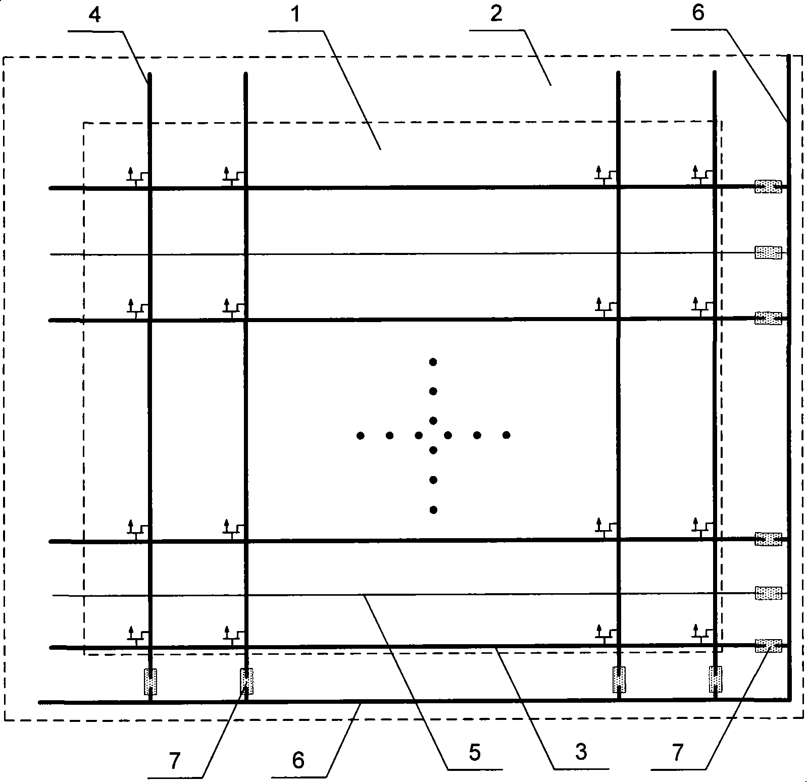
[0041] On the basis of the above-mentioned technical scheme, several common electrode lines 5 can also be formed in the display area 1, and joint points 7 can also be set between the common electrode lines 5 and the test lines 6, which are used to connect the test lines 6 and the common electrodes during testing. Line 5 is connected. Therefore, in this embodiment, the connection point 7 can be arranged at the end of the gate line 3, the data line 4 and / or the common electrode line 5, and is used to connect the test line 6 to the gate line 3 and connect the test line 6 to the data line during testing. 4. Connect and / or connect the test line 6 with the common electrode line 5.

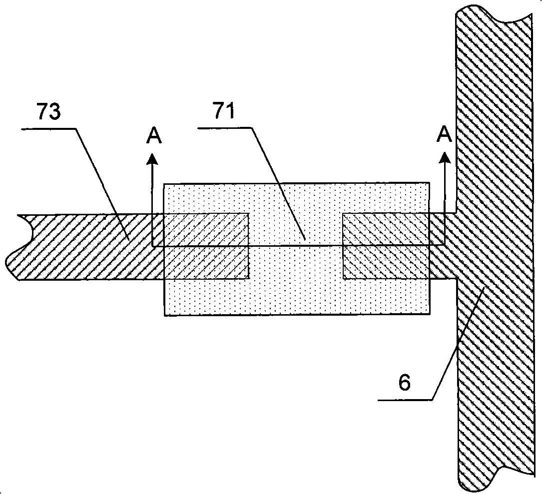
[0042] figure 2 It is a plan view of the bonding point in the TFT-LCD array substrate of the present invention. like figure 2 As shown, the main structure of the bonding point 7 includes a conductive connection layer 71, and the conductive connection layer 71 on the same layer as the pixel electrode...


PUM

PropertyMeasurementUnit
widthaaaaaaaaaa

Abstract

The invention relates to a TFT-LCD array substrate and methods for manufacturing and testing the same. The TFT-LCD array substrate comprises a display area and a peripheral area, wherein the display area is internally provided with a grid line and a data line, and the peripheral area is internally provided with a test line and a binding point for connecting the test line with the grid line and / orconnecting the test line with the data line. The method for testing the TFT-LCD array substrate comprises the following steps: connecting a signal line to be tested with the test line at the binding point in a laser welding way, and testing the signal line to be tested through the test line. Because the test line and the binding point are formed in the peripheral area, and the signal line to be tested is connected with the test line at the binding point in a laser welding way in the TFT-LCD array substrate testing process, a signal on the signal line can be tested, the test and analysis way ofthe liquid crystal panel can be strengthened and the comprehensive analysis ability of a TFT-LCD is improved.

Description

technical field [0001] The invention relates to a liquid crystal display device and its manufacturing method and testing method, in particular to a TFT-LCD array substrate and its manufacturing method and testing method. Background technique [0002] The main structure of a Thin Film Transistor Liquid Crystal Display (TFT-LCD) includes a liquid crystal panel, a backlight source and a driving circuit board. The liquid crystal panel consists of an array substrate, a color filter substrate and a liquid crystal layer disposed therebetween. The liquid crystal panel is a unity of opto-mechanical and electrical. Its basic principle is to use the electric field between the array substrate and the color filter substrate to control the deflection of liquid crystal molecules, so that it produces different transmitted light under different electric fields. As a unified whole, it can be considered that the liquid crystal panel is the load of the driving circuit, and the liquid crystal mo...

Claims


Application Information

Patent Timeline
Patent Type & Authority Patents(China)
IPC IPC(8): G02F1/13G02F1/1362H01L27/12H01L21/84
Inventor 张弥彭志龙
Owner K TRONICS (SUZHOU) TECH CO LTD
Why Eureka
Try Eureka