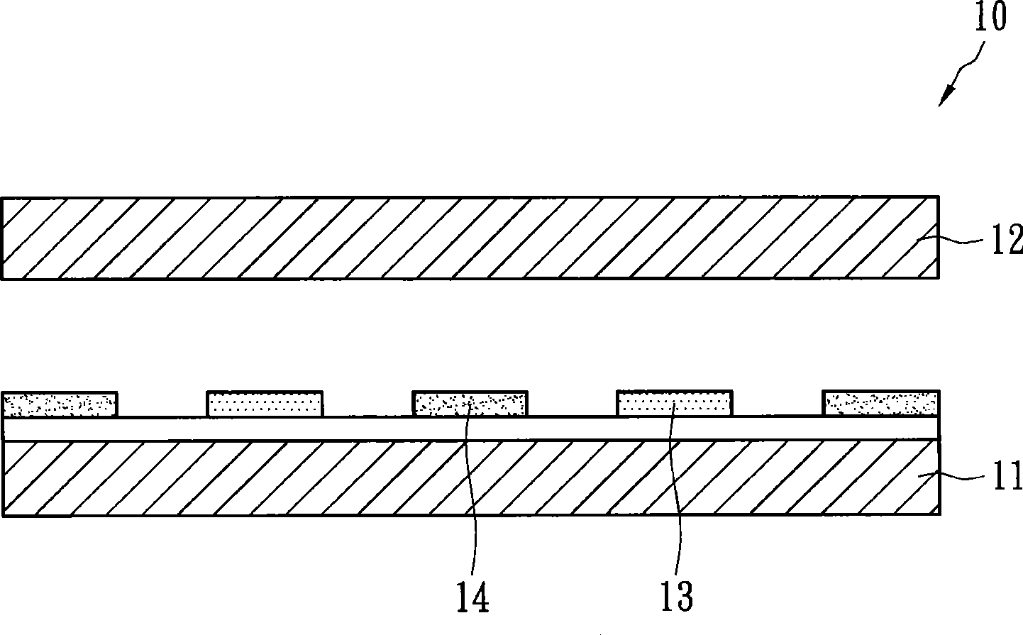
Liquid crystal display panel
A liquid crystal display panel and substrate technology, applied in nonlinear optics, instruments, optics, etc., can solve problems such as reducing transmittance, and achieve the effects of increasing light transmittance, reducing critical voltage, and improving display characteristics
- Summary
- Abstract
- Description
- Claims
- Application Information
AI Technical Summary
Problems solved by technology
Method used
Image
Examples
Embodiment Construction
[0041] The making and using of the presently preferred embodiment are discussed in detail below. It should be appreciated, however, that the present invention provides many applicable inventive concepts, which can be embodied in a wide variety of specific situations. The specific examples discussed are merely illustrative of specific ways to make and use the invention, and do not limit the scope of the invention.
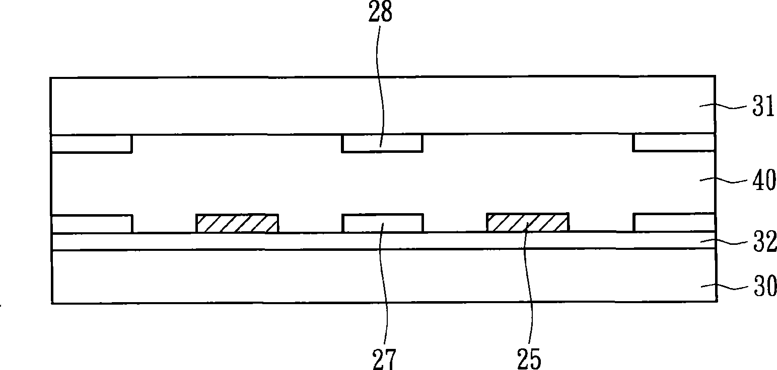
[0042] figure 2 A top view showing a liquid crystal display panel according to an embodiment of the present invention, image 3 yes figure 2 Sectional view along section line 1-1. The liquid crystal display panel 20 includes a first substrate 30 , a second substrate 31 and a liquid crystal layer 40 . The first substrate 30 is opposite to the second substrate 31 , and the liquid crystal layer 40 is between the first substrate 30 and the second substrate 31 . In the pixel unit of the liquid crystal display panel 20 , the scan lines (or called gate lines) 22 and...
PUM
 Abstract
Description
Claims
Application Information
 - R&D
- Intellectual Property
- Life Sciences
- Materials
- Tech Scout
- Unparalleled Data Quality
- Higher Quality Content
- 60% Fewer Hallucinations
Browse by: Latest US Patents, China's latest patents, Technical Efficacy Thesaurus, Application Domain, Technology Topic, Popular Technical Reports.
© 2025 PatSnap. All rights reserved.Legal|Privacy policy|Modern Slavery Act Transparency Statement|Sitemap|About US| Contact US: help@patsnap.com


