Liquid crystal device, method for producing the same, and electronic apparatus
A technology for liquid crystal devices and manufacturing methods, applied in nonlinear optics, instruments, optics, etc., capable of solving the problems of waste of materials for forming retardation films and complicated manufacturing processes, etc.
- Summary
- Abstract
- Description
- Claims
- Application Information
AI Technical Summary
Problems solved by technology
Method used
Image


Examples
Embodiment approach 1
[0075]
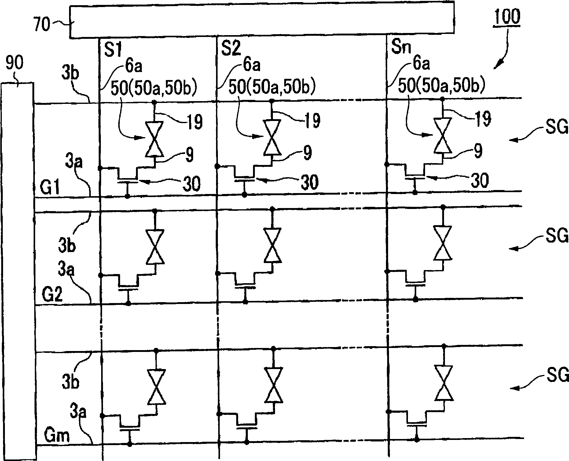
[0076] First, the liquid crystal device of this embodiment will be described. figure 1 is an equivalent circuit diagram showing the electrical configuration of the liquid crystal device.
[0077] Such as figure 1 As shown, the liquid crystal device 100 of this embodiment has a plurality of sub-pixels SG. Each sub-pixel SG has: a pixel electrode 9 ; a common electrode 19 ; and a TFT (Thin Film Transistor) 30 for switching and controlling the pixel electrode 9 . The liquid crystal layer 50 is located between the pixel electrode 9 and the common electrode 19 . The details of the liquid crystal layer 50 will be described later, and the liquid crystal layer 50 is divided into a first liquid crystal layer 50a and a second liquid crystal layer 50b. The common electrode 19 is electrically connected to the common line 3 b extending from the scanning line driver circuit 90 so as to be maintained at a common potential in each sub-pixel SG.
[0078] The data line 6 a extend...
Embodiment approach 2
[0127]
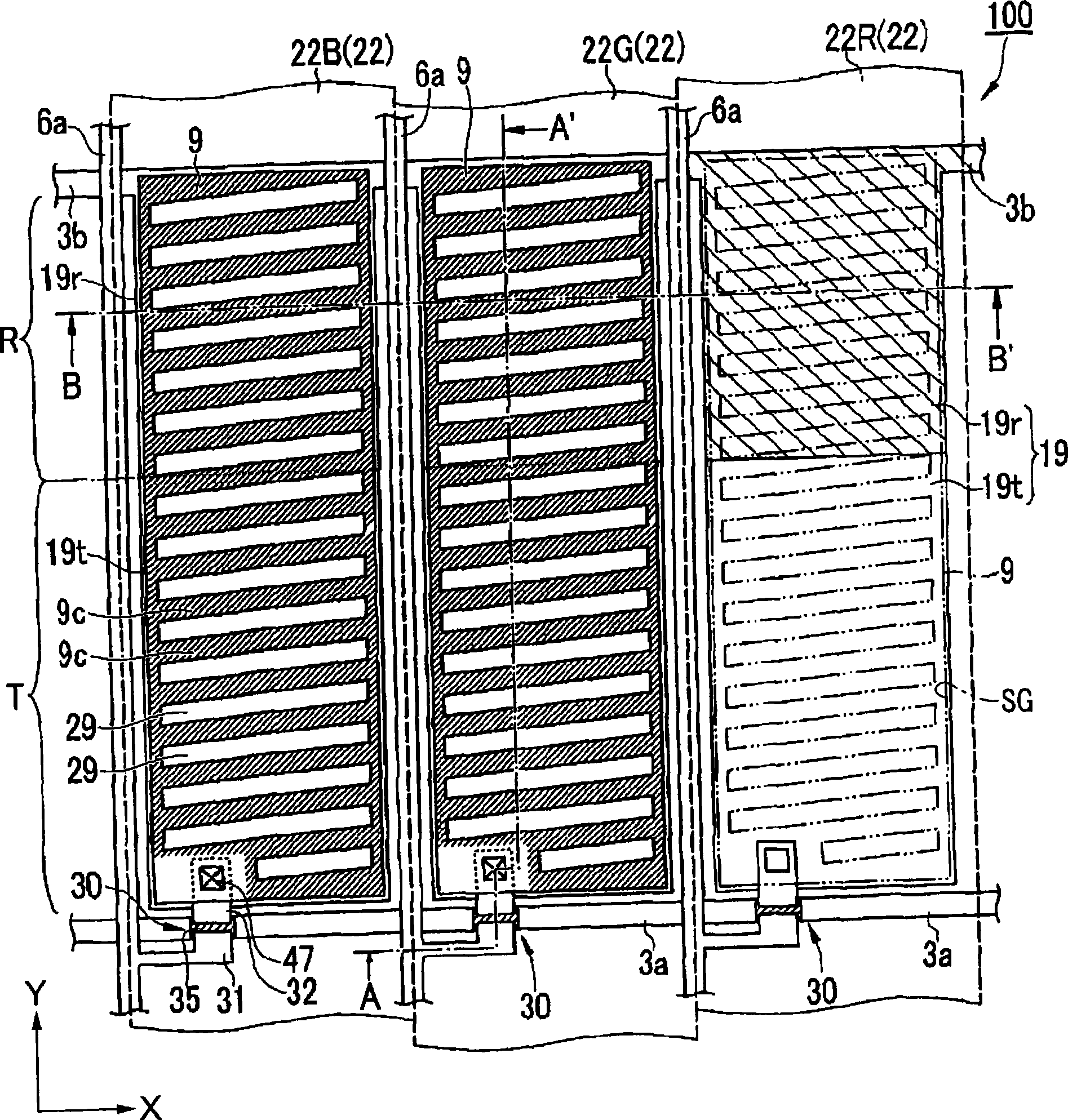
[0128] Next, the liquid crystal device of Embodiment 2 and its manufacturing method will be described with reference to the drawings. Figure 8 (a) and (b) are schematic cross-sectional views showing the structure of the liquid crystal device of the second embodiment. In addition, the same code|symbol is used for the part of the same structure as said Embodiment 1, and is demonstrated.
[0129] Such as Figure 8 As shown in (a), the liquid crystal device 200 of this embodiment further includes a liquid crystal layer thickness adjustment layer 25 ( 25G) for adjusting the thickness of the first liquid crystal layer 50 a in the reflective display region R compared to the first embodiment described above. The basic optical design conditions are the same as those of the liquid crystal device 100 in Embodiment 1, and the Figure 4 conditions shown.
[0130] The liquid crystal layer thickness adjustment layer 25 ( 25G ) is transparent and optically isotropic, and is lam...
Embodiment approach 3
[0151]
[0152] Next, a mobile phone as an electronic device according to the present embodiment will be described. Figure 11 It is a schematic perspective view showing a mobile phone as an electronic device.
[0153] Such as Figure 11 As shown, the mobile phone 300 of this embodiment has a main body including an input unit for operation and a display unit 301 . The display unit 301 incorporates the liquid crystal device 100 or the liquid crystal device 200 and an illumination device for illuminating the device. Accordingly, displayed information can be confirmed by transmissive display using transmitted light from the lighting device and reflective display using incident light such as external light. That is, in a sufficiently bright environment such as outdoors, information can be confirmed by reflective display without driving the lighting device. That is, the mobile phone 300 that saves power and has a long battery life is realized.
[0154]The mobile phone 300 is ...
PUM
 Abstract
Description
Claims
Application Information
 - R&D
- Intellectual Property
- Life Sciences
- Materials
- Tech Scout
- Unparalleled Data Quality
- Higher Quality Content
- 60% Fewer Hallucinations
Browse by: Latest US Patents, China's latest patents, Technical Efficacy Thesaurus, Application Domain, Technology Topic, Popular Technical Reports.
© 2025 PatSnap. All rights reserved.Legal|Privacy policy|Modern Slavery Act Transparency Statement|Sitemap|About US| Contact US: help@patsnap.com