Method for resetting image sensing and image sensing apparatus using the method

A technology for image sensing and reset signals, applied in image communication, color TV parts, TV system parts, etc., can solve the problems of increasing cost, power consumption, increasing noise, etc., and achieves long reset time , Avoid image delay, low power consumption and low noise

Active Publication Date: 2012-06-27
NOVATEK MICROELECTRONICS CORP
View PDF0 Cites 0 Cited by
  • Summary
  • Abstract
  • Description
  • Claims
  • Application Information

AI Technical Summary

Problems solved by technology

[0009] In addition to increasing cost and power consumption, the use of voltage pumping may also increase noise, such as: random noise, ripple noise and substrate noise, etc.

Method used


Image

  • Method for resetting image sensing and image sensing apparatus using the method
  • Method for resetting image sensing and image sensing apparatus using the method
  • Method for resetting image sensing and image sensing apparatus using the method

Examples


Embodiment Construction

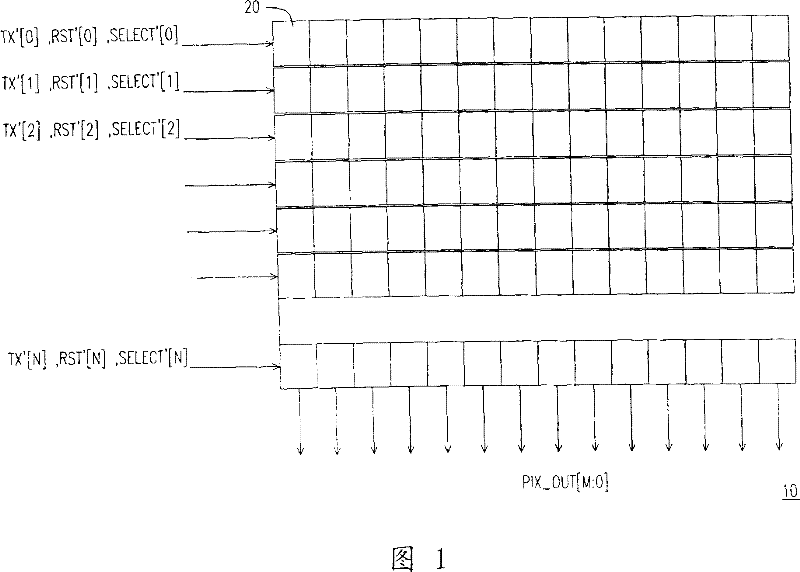
[0039]Embodiments of the present invention are characterized in that the pixel array is divided into a plurality of sections, and a block of pixel data is reset simultaneously to avoid image delay, and no voltage pumping is required.

[0040] Please refer to Figure 4 , Figure 4 is an embodiment circuit diagram of a pixel array 40 using the method of the present invention. Such as Figure 4 As shown, the pixel array 40 includes a plurality of image sensing units 6B0. This embodiment is a pixel array 40 of 16*16 pixels, and the pixel array 40 is divided into four pixel data blocks Sector0, Sector1, Sector2 and Sector3. The plurality of image sensing units 6B0 in row k of the pixel data block Sector x are controlled by the reset signal RST[k+4x], the control signal TX[k+4x] and the selection signal SELECT[k+4x], wherein, Both x and k are integers from 0 to 3. When the plurality of image sensing units 6B0 in each row of the pixel data block Sector0 perform exposure sensing ...


PUM


Abstract

The invention provides a method for resetting an image sensor and an image sensing device using the method. The method for resetting the image sensor comprises the following steps: generating a plurality of resetting signals and a plurality of control signals, and using the resetting signals and the control signals to control resetting and exposure sensing of a pixel array. The pixel array is provided with a plurality of pixel data blocks, and each pixel data block is provided with a plurality of pixel sensing units. When the plurality of the pixel sensing units of one pixel data block are exposed and sensed in turn to obtain a plurality of sensing signals, the plurality of the pixel sensing units of another pixel data block are reset.

Description

technical field [0001] The present invention relates to an image sensing method, and in particular to a reset method and an image sensing device applicable to a CMOS image sensor. Background technique [0002] With the progress of semiconductor and optoelectronic technology, more and more digital cameras, digital monitors or digital video cameras are flooding our lives. Photographic devices such as digital cameras, digital monitors, or digital video cameras require photosensitive elements to convert the sensed light signals into electrical signal outputs. Generally speaking, photosensitive elements are mostly charge coupled devices or complementary metal oxides. Semiconductor image sensing element (CMOS Image Sensor), although the image quality of CCD is better than that of CMOS image sensing element photography device, but the cost of CCD is higher than the cost of CMOS image sensing element, therefore, many electronic photography devices are still Using CMOS image sensing...

Claims


Application Information

Patent Timeline
Patent Type & Authority Patents(China)
IPC IPC(8): H04N5/374H04N5/3745
Inventor 周国煜
Owner NOVATEK MICROELECTRONICS CORP
Why Eureka
Try Eureka