Liquid crystal display device, and its manufacturing method
A technology of a liquid crystal display device and a manufacturing method, applied in nonlinear optics, instruments, optics, etc., can solve problems such as the inability to ensure the specified size of cell gaps
- Summary
- Abstract
- Description
- Claims
- Application Information
AI Technical Summary
Problems solved by technology
Method used
Image
Examples
Embodiment approach 1
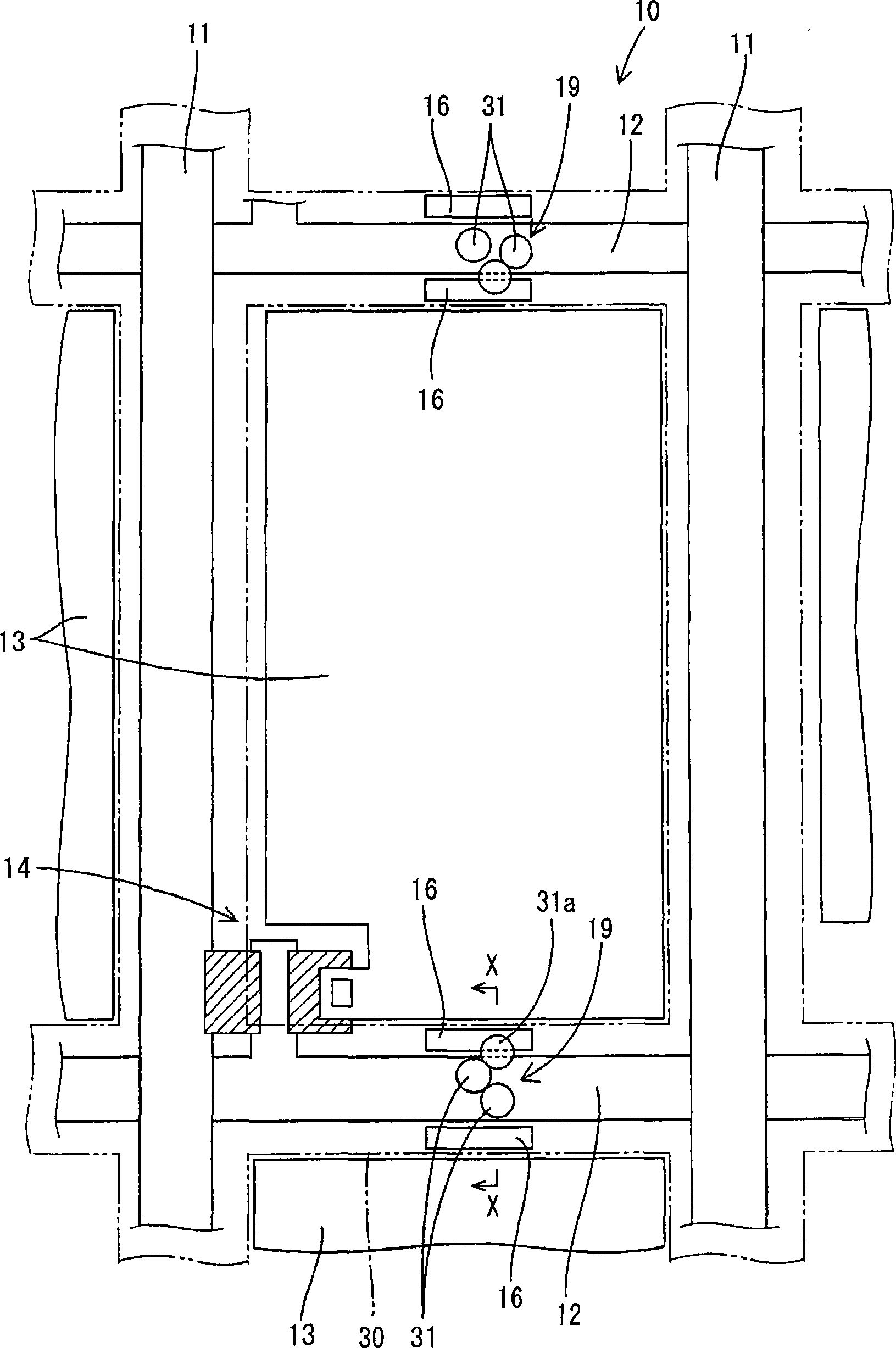
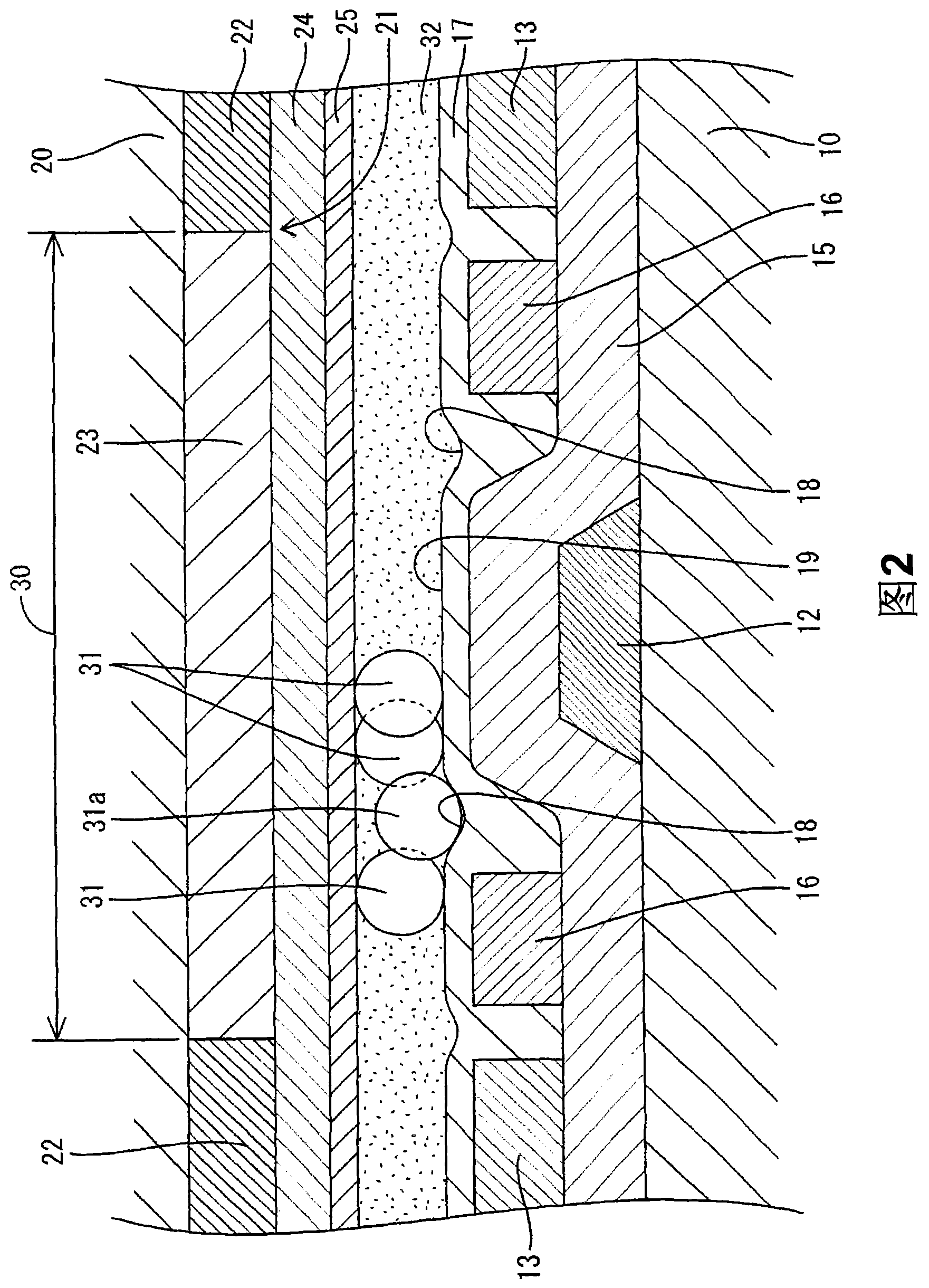
[0046] Below, refer to figure 1 with figure 2 Specific Embodiment 1 of the present invention will be described. The liquid crystal display device of the present embodiment is configured by stacking a pair of glass transparent substrates, that is, a TFT substrate 10 and a CF substrate 20 in parallel, and interposing spacer particles 31 between the two substrates 10 and 20 . While maintaining a constant distance (cell gap) between the two substrates 10 and 20 over the entire surface, liquid crystal 32 is filled in the gap between the two substrates 10 and 20 .
[0047] On the surface opposite to the TFT substrate 10 in the CF substrate 20, a color filter 21 is arranged, and the color filter 21 is arranged in a horizontal direction by a black light-shielding film 23 (black matrix) arranged in a grid shape and divided into a rectangular thin plate shape. The coloring part 22 of the three primary colors of red (R), green (G) and blue (B). In addition, a transparent thin-plate-...
Embodiment approach 2
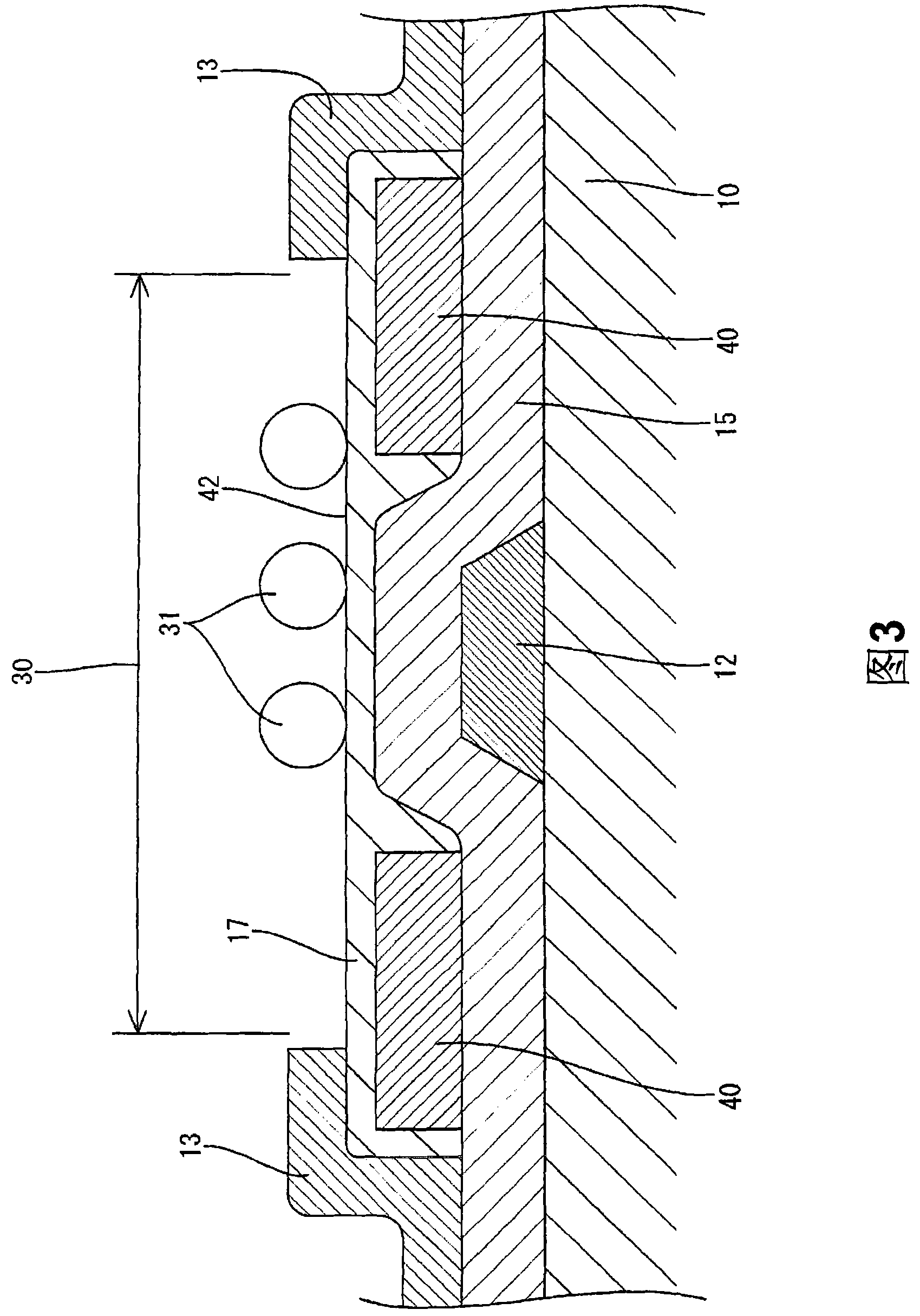
[0062] Below, refer to image 3 Embodiment 2 of the present invention will be described. The reinforcement layer 40 in the second embodiment is different from the first embodiment described above. The other configurations are the same as those in Embodiment 1, and therefore, the same symbols are attached to the same configurations, and descriptions of the configurations, operations, and effects are omitted.
[0063] The booster layer 40 of the second embodiment is made of the same material as the insulating layer provided on the TFT substrate 10 and the CF substrate 20 . Examples of the insulating layer include an i layer (a-Si: amorphous silicon) and an n+ layer (μC-Si: microcrystalline silicon). The width dimension of the booster layer 40 is larger than that of the booster layer 16 of Embodiment 1, and the edge portion of the booster layer 40 on the side opposite to the gate electrode line 12 protrudes outside the light shielding region 30 . Further, on the surface of the...
Embodiment approach 3
[0066] Below, refer to Figure 4 with Figure 5 Embodiment 3 of the present invention will be described. The third embodiment is different from the first embodiment described above in the placement surface 50 . The other configurations are the same as those of Embodiment 1 above, and therefore the same symbols are attached to the same configurations, and descriptions of the configurations, operations, and effects are omitted.
[0067] In Embodiment 3, a part of the gate electrode line 12 in the longitudinal direction is a substantially square wide portion 12W whose both side edges protrude outward. In the gate electrode line 12, the width dimension of the portion 12N other than the wide portion 12W is the same as in Embodiment 1, and narrower than the light shielding region 30, but the width dimension of the wide portion 12W is almost the same as that of the light shielding region 30 (than the width of the light shielding region 30 slightly smaller). In addition, on the su...
PUM
 Abstract
Description
Claims
Application Information
 - Generate Ideas
- Intellectual Property
- Life Sciences
- Materials
- Tech Scout
- Unparalleled Data Quality
- Higher Quality Content
- 60% Fewer Hallucinations
Browse by: Latest US Patents, China's latest patents, Technical Efficacy Thesaurus, Application Domain, Technology Topic, Popular Technical Reports.
© 2025 PatSnap. All rights reserved.Legal|Privacy policy|Modern Slavery Act Transparency Statement|Sitemap|About US| Contact US: help@patsnap.com


