Bus signal analysis tool for Flash storage chip

A bus signal and analysis tool technology, applied in the field of Flash memory chip bus signal analysis tools, can solve problems such as unsatisfactory, and achieve the effect of simple operation and large storage depth

Inactive Publication Date: 2009-03-11
INITIO HANGZHOU CORP
View PDF0 Cites 0 Cited by
  • Summary
  • Abstract
  • Description
  • Claims
  • Application Information

AI Technical Summary

Problems solved by technology

For the analysis of Flash memory chip bus signals using general signal test tools, it has been increasingly unable to meet such requirements

Method used


Image

  • Bus signal analysis tool for Flash storage chip
  • Bus signal analysis tool for Flash storage chip
  • Bus signal analysis tool for Flash storage chip

Examples


Embodiment Construction

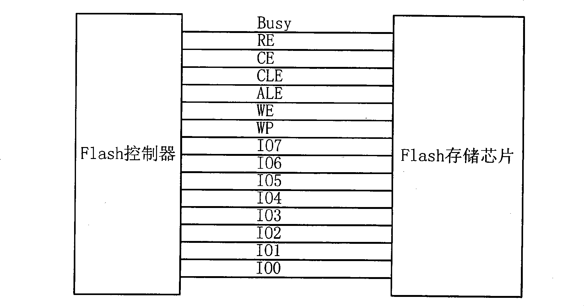
[0028] The application of the Flash storage chip bus signal analysis tool of the present invention is very simple, as long as the Flash bus signal sampling probe (such as connectors, wires, probes, etc.) of the present invention is directly connected to the corresponding Flash bus signal. That is to say, the present invention only needs to comprise two parts in the actual application:

[0029] (1) The analyzed objects related to the Flash memory chip.

[0030] (2) Flash bus signal analysis tool.

[0031] In order to achieve such requirements, the Flash bus signal analysis tool must have the following five functions:

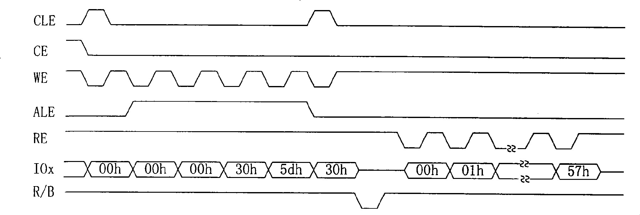
[0032] (1) Sampling the Flash bus signal of the analyzed object, the Flash bus signal analysis tool is connected to the Flash bus signal of the analyzed object through sampling probes (such as connectors, wires, probes, etc.), and according to a certain frequency ( Generally greater than 2 times the frequency of the Flash bus) to sample it.

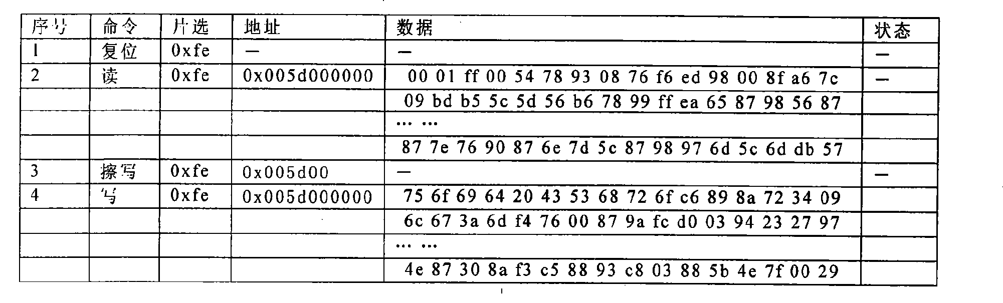
[0033] (2) Analyz...


PUM


Abstract

The invention discloses a bus signal analyzing tool of a Flash storage chip, which comprises a Flash bus signal sampling unit, a Flash bus signal analyzing unit, a Flash bus signal display unit, a Flash bus signal storage unit and a Flash erasing harmony analyzing unit, wherein the Flash bus signal sampling unit, the Flash bus signal display unit, the Flash bus signal storage unit and the Flash erasing harmony analyzing unit are respectively connected with the Flash bus signal analyzing unit, and the Flash bus signal storage unit and the Flash erasing harmony analyzing unit are respectively connected with the Flash bus signal display unit. Compared with the traditional testing tool, in the aspect of analyzing bus signals of the Flash storage chip, the invention has great progress and obvious advantages, the building and analyzing environment is very simple, the operation is simple and convenient, and the storage depth is large.

Description

technical field [0001] The invention relates to products related to Flash memory chips, in particular to a bus signal analysis tool for Flash memory chips. Background technique [0002] Flash memory chips are widely used in various fields, such as SD cards, U disks, SSD hard disks, etc. These Flash memory chip-related products all involve Flash bus signals. The Flash bus signal refers to: the collection of all control and data signals on the Flash memory chip, such as figure 1 Shown is an application model of a Flash memory chip. It can be seen from the figure that the Flash controller is connected to the Flash memory chip through a group of buses, and this group of buses is the Flash bus. Among them, I00~I07 are data signal lines, and the Flash controller sends commands, addresses, data and receive data to the Flash memory chip through these data signal lines; CE, Busy, ALE, CLE, WP, WE, RE are the Flash controller and the Flash Control signal lines between memory chips...

Claims


Application Information

Patent Timeline
Patent Type & Authority Applications(China)
IPC IPC(8): G11C29/00G11C29/56
Inventor 骆建军陶航陈丽娜
Owner INITIO HANGZHOU CORP
Why Eureka
Try Eureka