
Method and circuit for loading on site programmable gate array

A technology of loading circuits and gate arrays, applied in the direction of program loading/starting, program control devices, etc., can solve the problems of limited clock rate control time, large data loading speed limit, affecting system initialization work, etc., to reduce the startup configuration. time, improve product performance and indicators, and reduce the effect of failure recovery time

Inactive Publication Date: 2009-01-28
COMBA TELECOM SYST CHINA LTD
View PDF0 Cites 15 Cited by
  • Summary
  • Abstract
  • Description
  • Claims
  • Application Information

AI Technical Summary

Problems solved by technology

[0008] Since this loading method needs to control the working status of each pin through software, the software control method usually has an upper limit threshold for the highest transmission rate, so the data loading speed is limited. At the same time, the control time of GPIO pins is limited by the MCU. For example, loading data uses software to control the ARM instruction clock and data transmission of the digital board. The loading time of the FPGA is limited by the instruction clock of the MCU, and the ARM instruction clock of the digital board usually controls the clock for loading the FPGA to about 500K
Moreover, to load a byte of data, you need to control the CCLK and D_IN pins eight times respectively. For FPGA data that loads large files, the loading time is difficult to control, and even the loading time is too long, which affects the system initialization.

Method used


Image

  • Method and circuit for loading on site programmable gate array
  • Method and circuit for loading on site programmable gate array
  • Method and circuit for loading on site programmable gate array

Examples


Embodiment Construction

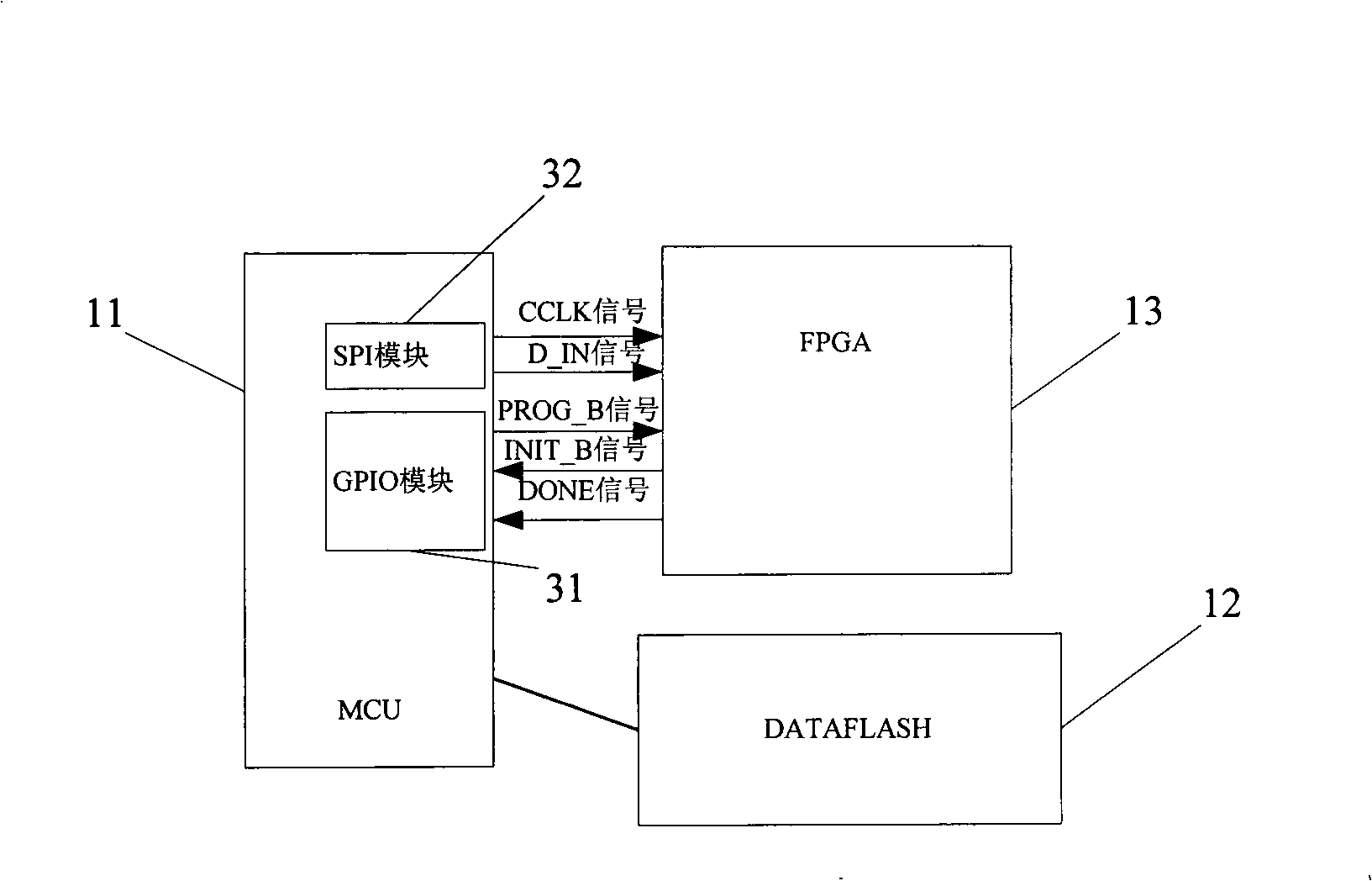
[0025] refer to figure 2 and image 3 , the present invention uses SPI (Serial Peripheral Interface, serial bus transmission interface) to the loading method and loading circuit of FPGA loading data to overcome the speed requirement to MCU pin. Such as image 3 As shown, MCU 11 is connected with FPGA 13 through GPIO 31 module and SPI 32 module. In one embodiment, the MCU 11 is connected to the DATAFLASH 12 through the bus, so as to quickly load the files stored in the DATAFLASH 12 to the FPGA 13 through the GPIO 31 module and the SPI32 module.

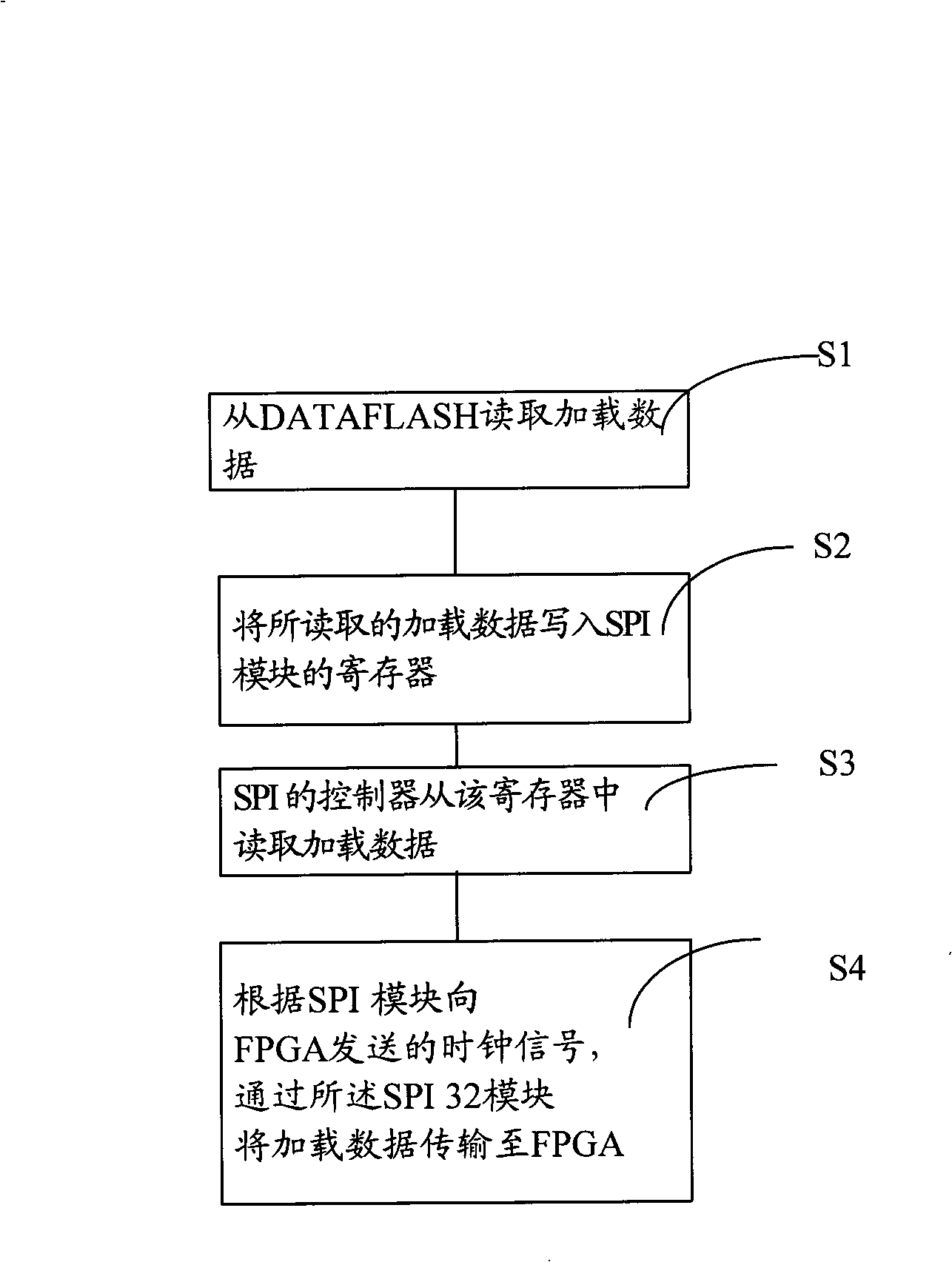
[0026] Such as figure 2 As shown, when loading data to FPGA 13, MCU 11 reads loading data (S1) from DATAFLASH12; Then writes the loading data read in the register of SPI 32 module (S2); The controller of SPI reads from this register In the present invention, send clock signal to FPGA 13 by SPI 32 module, according to the clock signal that SPI 32 module sends to FPGA 13, load data is transmitted to FPGA 13 by described SPI 32 modu...


PUM


Abstract

The invention provides a loaded circuit for a field programmable gate array and a loading method thereof. The loaded circuit comprises a microprocessor, a nonvolatile memory and the field programmable gate array, wherein the nonvolatile memory is connected with the microprocessor, and the microprocessor is connected with the field programmable gate array. When the loaded circuit is used to load data, the microprocessor reads and loads data from the nonvolatile memory and writes the loaded data in a register; and the loaded data is read from the register by a controller and is transmitted to the field programmable gate array through a loaded digital signal. The loaded circuit can improve the speed of the whole loading process and greatly reduce the loading time, thereby reducing the system starting and configuration time and the system fault recovery time, and improving the product performance and indexes.

Description

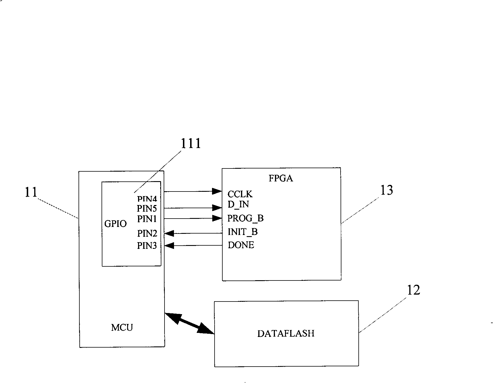
technical field [0001] The invention relates to a method for loading files into a field programmable gate array and a corresponding loading circuit. Background technique [0002] FPGA (Field-programmable gate arrays, Field Programmable Gate Array) is an erasable and programmable read-only memory. Usually, when the board is powered on and initialized, relevant program data is loaded into the FPGA. After the FPGA is initialized, it can complete complex logic control and realize various business processing functions. Since the FPGA is a logic chip that does not save data after power-off, it is required to reload after each power-on, that is, to reload the program data and write it into the FPGA chip so that it can work normally. [0003] See figure 1 , figure 1 It is a kind of existing loading circuit to FPGA loading file, and this circuit comprises microprocessor (MCU) 11, non-volatile memory DATAFLASH 12 and FPGA 13, and non-volatile memory 12 is connected with MCU 11, an...

Claims


Application Information

Patent Timeline
IPC IPC(8): G06F9/445
Inventor 左延麟
Owner COMBA TELECOM SYST CHINA LTD
Learn More