
Method for depositing atomic layer and semiconductor device formed by the same

一种原子层沉积、半导体的技术,应用在半导体器件、半导体/固态器件制造、电固体器件等方向,能够解决原子岛尺寸分布均匀性差等问题,达到原子尺寸大小均匀一致的效果

Active Publication Date: 2008-12-24
SEMICON MFG INT (SHANGHAI) CORP +1
View PDF1 Cites 10 Cited by
  • Summary
  • Abstract
  • Description
  • Claims
  • Application Information

AI Technical Summary

Problems solved by technology

However, in the prior art, methods for forming discrete atomic islands (nano-dots) to trap charge layers generally use chemical vapor deposition or physical vapor deposition, and the size of the formed atomic islands is between 10nm and 100nm, and the size of the atomic islands is Poor distribution uniformity

Method used


Image

  • Method for depositing atomic layer and semiconductor device formed by the same
  • Method for depositing atomic layer and semiconductor device formed by the same
  • Method for depositing atomic layer and semiconductor device formed by the same

Examples


Embodiment 1

[0053] This embodiment provides an atomic layer deposition method, refer to the attached Figure 13 The shown process flow chart comprises the following steps:

[0054] Step S200, placing a semiconductor substrate in the atomic layer deposition chamber;

[0055] Step S201, the first precursor gas flows to the semiconductor substrate in the atomic layer deposition chamber to form a discretely distributed first monolayer on the semiconductor substrate;

[0056] Step S202, the inert purge gas flows to the atomic layer deposition chamber to remove the first precursor gas that does not form the first monolayer;

[0057] Step S203, the second precursor gas flows to the atomic layer deposition chamber, and reacts with the first precursor gas forming the first monolayer to form a discrete first compound monolayer;

[0058] Step S204, the inert purge gas flows to the atomic layer deposition chamber to remove the second precursor gas that has not reacted with the first precursor gas a...

Embodiment approach

[0085] As a specific implementation manner, the second precursor gas may be a substance containing N atoms or O atoms or metal atoms, used as a reducing agent or an oxidizing agent. The substance containing N atoms or O atoms or metal atoms is, for example, NH 3 or O 2 .

[0086] Just as an example, this embodiment provides several specific second precursor gases, so that those skilled in the art can better understand and implement the present invention. If the finally formed discrete distribution of the first compound monolayer is Si 3 N 4 , then the first precursor gas is a reaction gas with a Si atom nucleating body substance, and the second precursor gas is a gas capable of reacting with the first monolayer nucleating body formed by the first precursor gas to form a compound monolayer, By way of example only, the second precursor gas could be NH 3 , N 2 O, N 2 Wait for gas.

[0087] If the finally formed discrete distribution of the first compound monolayer is SiO ...

Embodiment 2

[0129] This embodiment provides an atomic layer deposition method, refer to the attached Figure 20 Process flow chart, including the following steps:

[0130] Step S300, placing a semiconductor substrate in the atomic layer deposition chamber;

[0131] Step S301, the first precursor gas flows to the semiconductor substrate in the atomic layer deposition chamber to form a discretely distributed first monolayer on the semiconductor substrate;

[0132] Step S302, the inert purge gas flows to the atomic layer deposition chamber to remove the first precursor gas that does not form the first monolayer;

[0133] Step S303, the second precursor gas flows to the atomic layer deposition chamber, and reacts with the first precursor gas forming the first monolayer to form a discrete first compound monolayer;

[0134] Step S304, the inert purge gas flows to the atomic layer deposition chamber to remove the second precursor gas that has not reacted with the first monolayer and by-product...


PUM

PropertyMeasurementUnit
sizeaaaaaaaaaa

Abstract

The invention relates to an atomic layer deposition (ALD) method which includes the steps as follows: first precursor gas flows to a semiconductor substrate in an atomic layer deposition room and a first scattered monolayer is formed; inert purge gas flows to the semiconductor substrate in the atomic layer deposition room; second precursor gas flows into the atomic layer deposition room and reacts with the first precursor gas that forms the first monolayer and a first scattered compound monolayer is formed; the inert purge gas flows into the atomic layer deposition room; and a second scattered compound monolayer is formed on the semiconductor substrate by referring to the technique which forms the first scattered compound monolayer. The method forms the first scattered compound monolayer and the second compound monolayer on the semiconductor substrate. The invention also provides a semiconductor device and the charge trap layer of the semiconductor device is a dielectric layer which contains the first scattered compound monolayer and the second compound monolayer formed by adopting an atomic deposition method.

Description

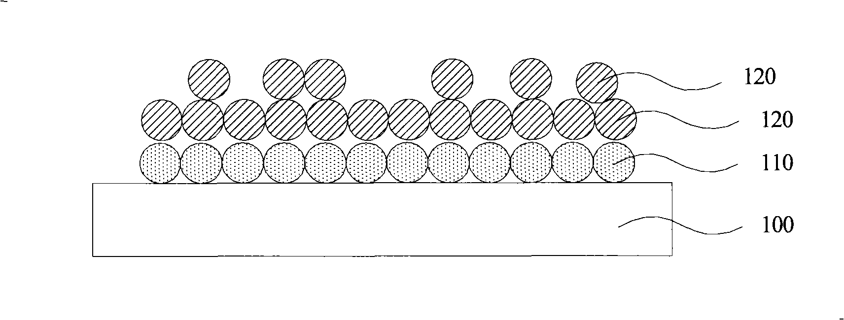
technical field [0001] The invention relates to the technical field of semiconductor manufacturing, in particular to an atomic layer deposition method and a formed semiconductor device. Background technique [0002] Atomic Layer Deposition (ALD), originally called Atomic Layer Epitaxy (ALE), is also called Atomic Layer Chemical Vapor Deposition (ALCVD). [0003] Atomic layer deposition (ALD) involves the deposition of successive monolayers onto a semiconductor substrate in a deposition chamber that is typically maintained at negative pressure (pressure below atmospheric pressure). A representative method is as disclosed in the background technology of the Chinese patent application document with the application number 03818269, including: refer to the attached figure 1 As shown, the first vaporized precursor is supplied into the deposition chamber to effectively form the first monolayer 110 on the semiconductor substrate 100 placed in the deposition chamber. Then, refer to...

Claims


Application Information

Patent Timeline
Patent Type & Authority Applications(China)
IPC IPC(8): H01L21/285H01L21/336H01L29/792C30B25/14C23C16/455
CPCC23C16/45529H01L29/40117H01L21/0228H01L21/0217H01L21/0214H01L21/02211H10B43/00H01L21/3185H01L21/318H01L21/3141H01L21/31645
Inventor 季华季明华三重野文健
Owner SEMICON MFG INT (SHANGHAI) CORP
Learn More