
Independent MO source pipe line of semiconductor material growth apparatus and application thereof

A semiconductor and pipeline technology, applied in the field of metal organic chemical vapor phase epitaxy MOCVD growth equipment, can solve the problems of contamination, increasing the difficulty of AlGaN, and the difficulty of realizing AlGaN materials with high Al composition

Inactive Publication Date: 2010-09-08
NANJING UNIV
View PDF0 Cites 0 Cited by
  • Summary
  • Abstract
  • Description
  • Claims
  • Application Information

AI Technical Summary

Problems solved by technology

[0015] The problem to be solved by the present invention is: in the MOCVD system, there are many differences in the growth mechanisms of AlGaN and GaN during the growth process, one of the main manifestations is that when growing AlGaN materials with high Al composition, due to TMAl will mix with NH 3 Factors such as strong parasitic reactions of the reactants in the sample cause many Al atoms to be consumed before they diffuse to the surface of the sample to participate in the growth, which increases the difficulty of controlling the composition of AlGaN, especially for AlGaN with high Al composition. The material is difficult to realize, which makes the development of the device difficult; and the retention of TMAl in the transportation pipeline will bring contamination to the system and other metal organic sources

Method used


Image

  • Independent MO source pipe line of semiconductor material growth apparatus and application thereof
  • Independent MO source pipe line of semiconductor material growth apparatus and application thereof

Examples


Embodiment Construction

[0023] Chemical Vapor Deposition CVD technology is a method that utilizes gas-phase chemical reaction to form the required epitaxial film. It transports several gases containing the chemical composition of thin film elements to the surface of the substrate through an inner polished stainless steel tube, and uses different heating methods, such as resistance wire heating, radio frequency heating, light heating, etc., to promote gas phase reaction or surface phase reaction. reaction, the reaction product is deposited on the substrate surface to form an epitaxial film. Metal-organic chemical vapor deposition (MOCVD) technology is a CVD technology that transports metal elements in compound semiconductors to the surface in the form of metal-organic MO sources. The MO source usually uses trimethylgallium TMGa, trimethylaluminum TMAl, trimethylindium TMIn as the Group III metal source, NH 3 As a source of group V nitrogen. For the growth of III-nitride binary alloys, the chemical r...


PUM


Abstract

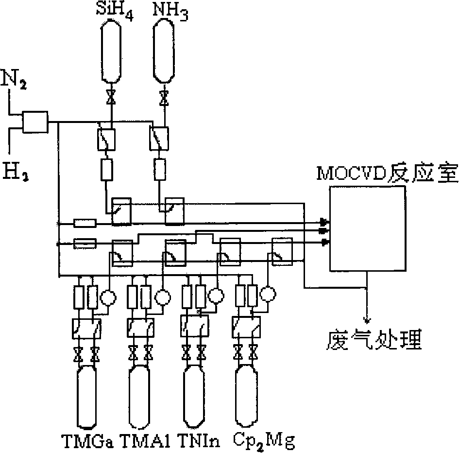
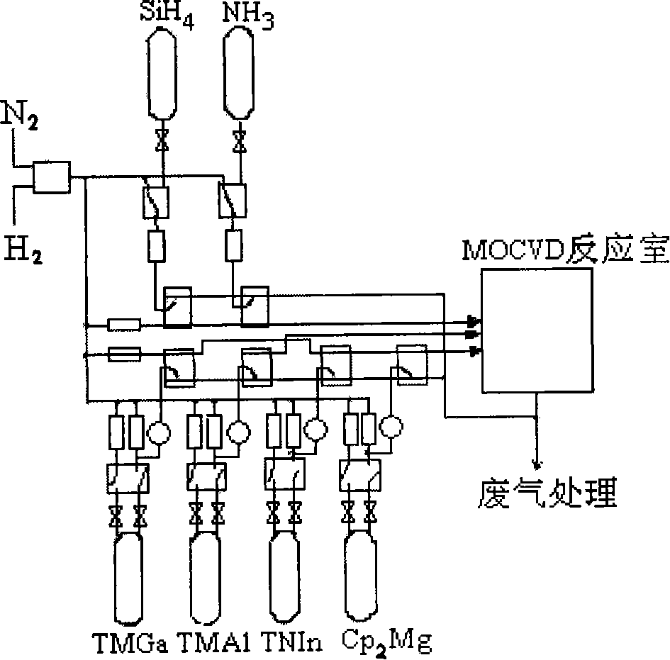
The invention relates to an independent MO source pipeline of a semiconductor material growth apparatus, and the application. Three or four or five inlet pipelines are provided, wherein, one pipeline is a V- nitrogen source pipeline, one pipeline is a 3-metal source mixing pipeline, other pipelines are independent 3-metal source pipelines, and all different source pipelines are then mixed with other reactant sources directly when closing to a reaction chamber. Through the method for independently designing the 3-metal source pipelines which take place side reactions easily such as a TMA1 source, etc., the independent MO source pipeline thoroughly solves the reaction detention of the metal sources in the equipment pipelines, the pollution to other MO sources, and the predecomposition mixing during the pipeline transporting process, and is especially suitable for a UV-LED, a AlGaN of a UV-LD, and a MOCVD equipment system of relative material growth, and can be used on all semiconductor material growth apparatuses such as a CVD, a HVPE, a MBE, etc., which use the MO sources. The independent MO source pipeline is not applied to the semiconductor material growth apparatus which is usedat present.

Description

technical field [0001] The invention relates to the technical field of metal organic chemical vapor phase epitaxy MOCVD growth equipment, which is an independent MO source pipeline and application of semiconductor material growth equipment, and can be used for all CVD, HVPE and MBE using volatile high-purity metal organic MO source and other semiconductor material growth equipment. Background technique [0002] At the end of the last century, with breakthroughs in material quality and p-type doping, the research and application of GaN-based semiconductor materials have made breakthroughs, and their blue-green light-emitting diodes (LEDs) and lasers (LDs) have been successfully commercialized. [1,2] . At present, white lighting caused by GaN-based LEDs has become a focus industry all over the world. Commercial products such as blue and green light-emitting diodes (LEDs) and laser diodes (LDs) illustrate the potential of III-V elements. [0003] Chemical vapor deposition CV...

Claims


Application Information

Patent Timeline
Patent Type & Authority Patents(China)
IPC IPC(8): C23C16/34H01L21/00
Inventor 谢自力张荣陈鹏刘斌李弋韩平修向前陆海江若琏施毅郑有炓
Owner NANJING UNIV
Learn More