Semiconductor device and test mode control circuit

A test mode, semiconductor technology, applied in the direction of measuring electricity, measuring devices, measuring electrical variables, etc., can solve problems such as release, inability to ensure safety, and reduced LSI yield.

Inactive Publication Date: 2008-08-27
PANASONIC CORP
View PDF1 Cites 2 Cited by
  • Summary
  • Abstract
  • Description
  • Claims
  • Application Information

AI Technical Summary

Problems solved by technology

[0012] However, there is a problem in the above-mentioned prior art that the test mode is prohibited only when the data of the test mode control flag stored in the nonvolatile memory matches the specific test mode prohibition code, so even if it is not Even if the data of the test mode control flag stored in the volatile memory changes only by 1 bit due to a fault, the prohibition of the test mode is also released.
As a result, when shifting to the test mode, data that requires security such as an authentication code can be accessed, so the possibility of circuit information being leaked or tampered with increases, and security cannot be ensured
[0013] On the other hand, the problem that also exists is: if adopt the mode that forbids the test mode under the inconsistent situation of the data of the test mode control sign that only stores in the non-volatile memory and specific test mode prohibiting sign indicating number, then when not determining just In the case of manufactured non-volatile memory data, there are a large number of LSIs whose test mode is disabled after manufacture
If the test mode is disabled after the manufacturing is completed, the initialization of the non-volatile memory cannot be performed, which will lead to a decrease in the yield of the LSI

Method used


Image

  • Semiconductor device and test mode control circuit
  • Semiconductor device and test mode control circuit
  • Semiconductor device and test mode control circuit

Examples


Embodiment 1

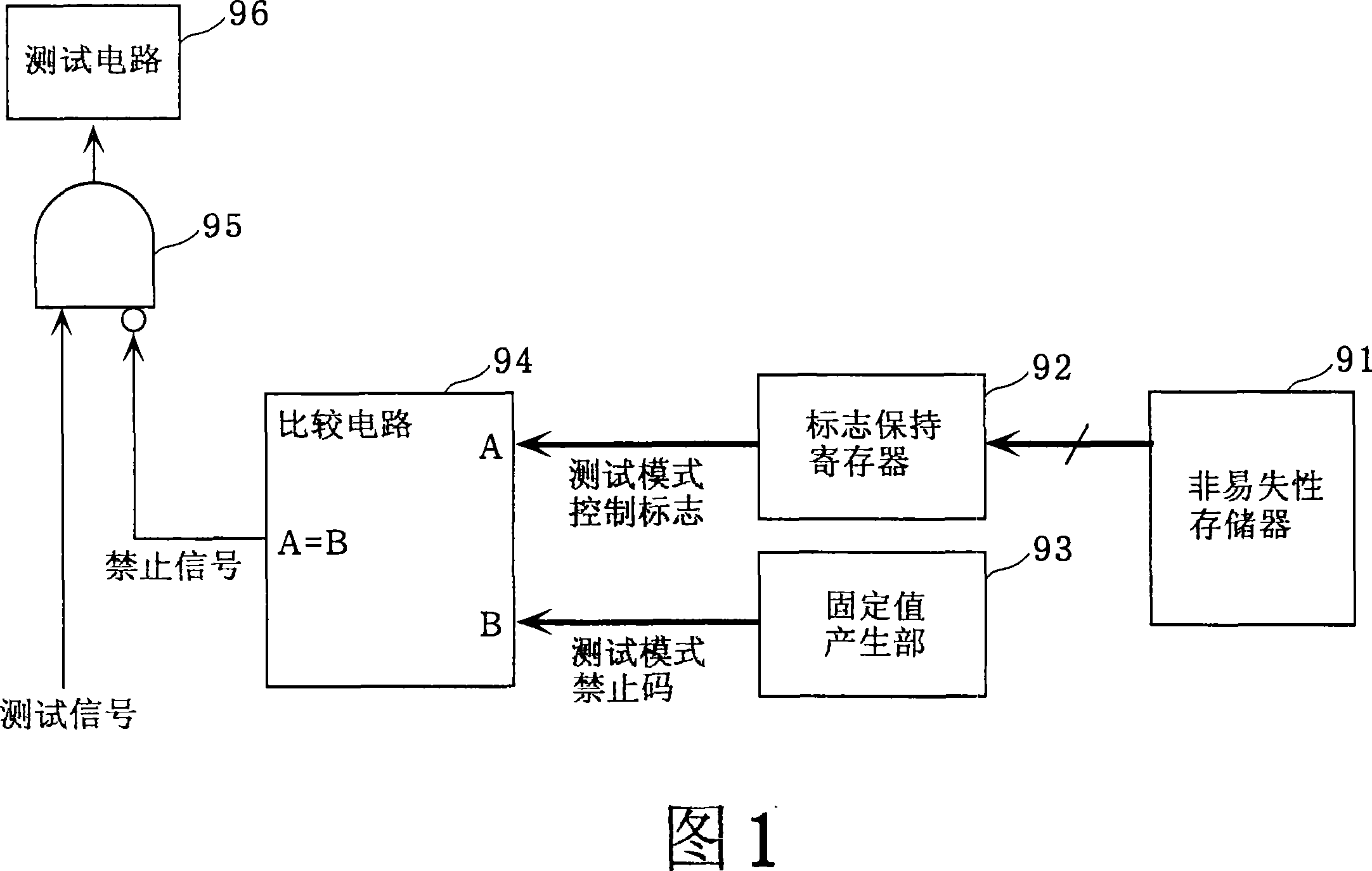
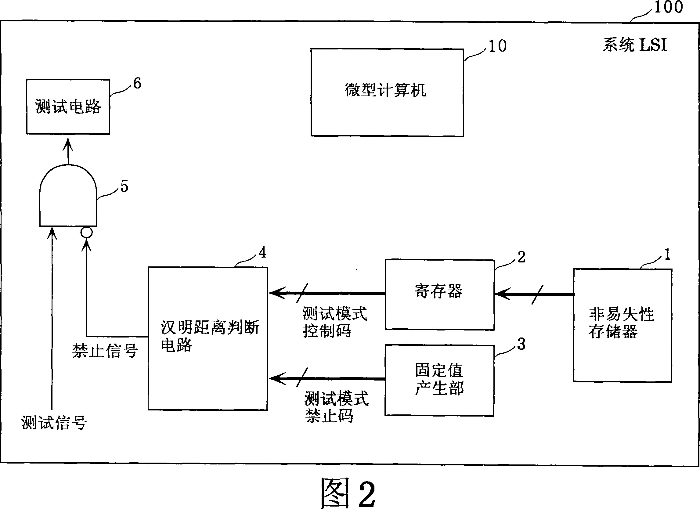
[0057] FIG. 2 is a block diagram of a system LSI having a test mode control circuit in Embodiment 1 of the present invention. In this figure, the system LSI 100 is a semiconductor device with a test mode, including a nonvolatile memory 1, a register 2, a fixed value generator 3, a Hamming distance judgment circuit 4, an AND circuit 5, a test circuit 6, and a micro computer10. Furthermore, a test mode control circuit is constituted by part of the nonvolatile memory 1 , the register 2 , the fixed value generator 3 , the Hamming distance judgment circuit 4 , and the AND circuit 5 .

[0058] The nonvolatile memory 1 stores a test mode control code for enabling or prohibiting transition to the test mode at a predetermined address. The test mode control code is set as necessary immediately after the factory manufactures or during maintenance. After shipment, a test mode control code for prohibiting transition to the test mode is set.

[0059] The register 2 holds the test mode in...

Embodiment 2

[0086] 8 is a block diagram showing the structure of a semiconductor device in Embodiment 2 of the present invention. This figure is different from FIG. 2 in that a selector 7 is added, and an output signal from the selector 7 is input to the register 2 . Hereinafter, the difference will be mainly explained, and the same point will be omitted.

[0087]The selector 7 receives the test mode control code from the nonvolatile memory 1 and the fixed value from the fixed value generator 3, selects the test mode control code when the reset signal is active, and selects the fixed value when the reset signal is invalid.

[0088] The selector 7 holds a fixed value as an initial value when the semiconductor device is reset, and holds the test mode control code from the nonvolatile memory 1 after the reset.

[0089] According to this, the Hamming distance judging circuit 4 asserts the prohibition signal during the period from reset until the test mode control code is set in the register,...

Embodiment 3

[0092] 9 is a block diagram showing the structure of a semiconductor device in Embodiment 3 of the present invention. This figure is different from FIG. 2 in that an access circuit 8 is added. Hereinafter, the difference will be mainly explained, and the same point will be omitted.

[0093] The flag access circuit 8 is a hardware circuit that performs the work shown in FIG. 4 or FIG. 7 . That is, the access circuit 8 automatically generates a read signal for the address storing the test mode control code of the nonvolatile memory 1 after the reset signal is input, and writes it into the register 2 . After the writing of the test mode control code is finished, when the Hamming distance judging circuit 4 outputs a high level and the Hamming distance is 1 or more, that is, the test mode control code stored in the nonvolatile memory 1 When the Hamming distance from the test mode inhibit code is less than or equal to a predetermined number and the number of bits of the test mode ...


PUM


Abstract

A semiconductor device is provided in which its security is fully ensured and its manufacturing yield is not lowered even if a data bit change occurs due to a malfunction or the like in the test mode control flag data stored in a nonvolatile memory. The semiconductor device comprises a nonvolatile memory (1) for storing a test mode control code into a predetermined address, a generator (3) for generating a fixed value indicating whether the test mode is disabled or enabled, and a Hamming distance decision circuit (4) for controlling the transfer to the test mode depending on whether the Hamming distance between the control code and the fixed value is less than or equal to a predetermined value or not.

Description

technical field [0001] The present invention relates to a semiconductor device having a test mode, and more particularly to a test mode control technique for a semiconductor device requiring safety. Background technique [0002] For LSI (Large Scale Integration: Large Scale Integration) loaded with highly confidential data or programs, and LSIs loaded with security circuits for IC cards, etc., to prevent leakage and falsification of data, programs, and circuit information using test patterns , it is required that the test mode cannot be used after the product is shipped. [0003] The methods for prohibiting the test mode include: comparing the test mode control flag with specific comparison data, allowing the test mode when they are consistent, and prohibiting the test mode when they are inconsistent. The test mode control flag shows the value of the test mode Enforcement is allowed or prohibited. The test mode control flag is stored in a predetermined address in the nonvo...

Claims


Application Information

Patent Timeline
Patent Type & Authority Applications(China)
IPC IPC(8): G01R31/28
CPCG01R31/31701G01R31/31719
Inventor 吉冈和树
Owner PANASONIC CORP
Why Eureka
Try Eureka