A FPGA-based multi-functional communication interface conversion device and method
A technology of communication interface and conversion equipment, applied in the fields of information communication and electronic information, can solve the problem of non-uniform communication interface, and achieve the effect of flexible application, perfect function and high degree of integration
- Summary
- Abstract
- Description
- Claims
- Application Information
AI Technical Summary
Problems solved by technology
Method used
Image
Examples
Embodiment Construction
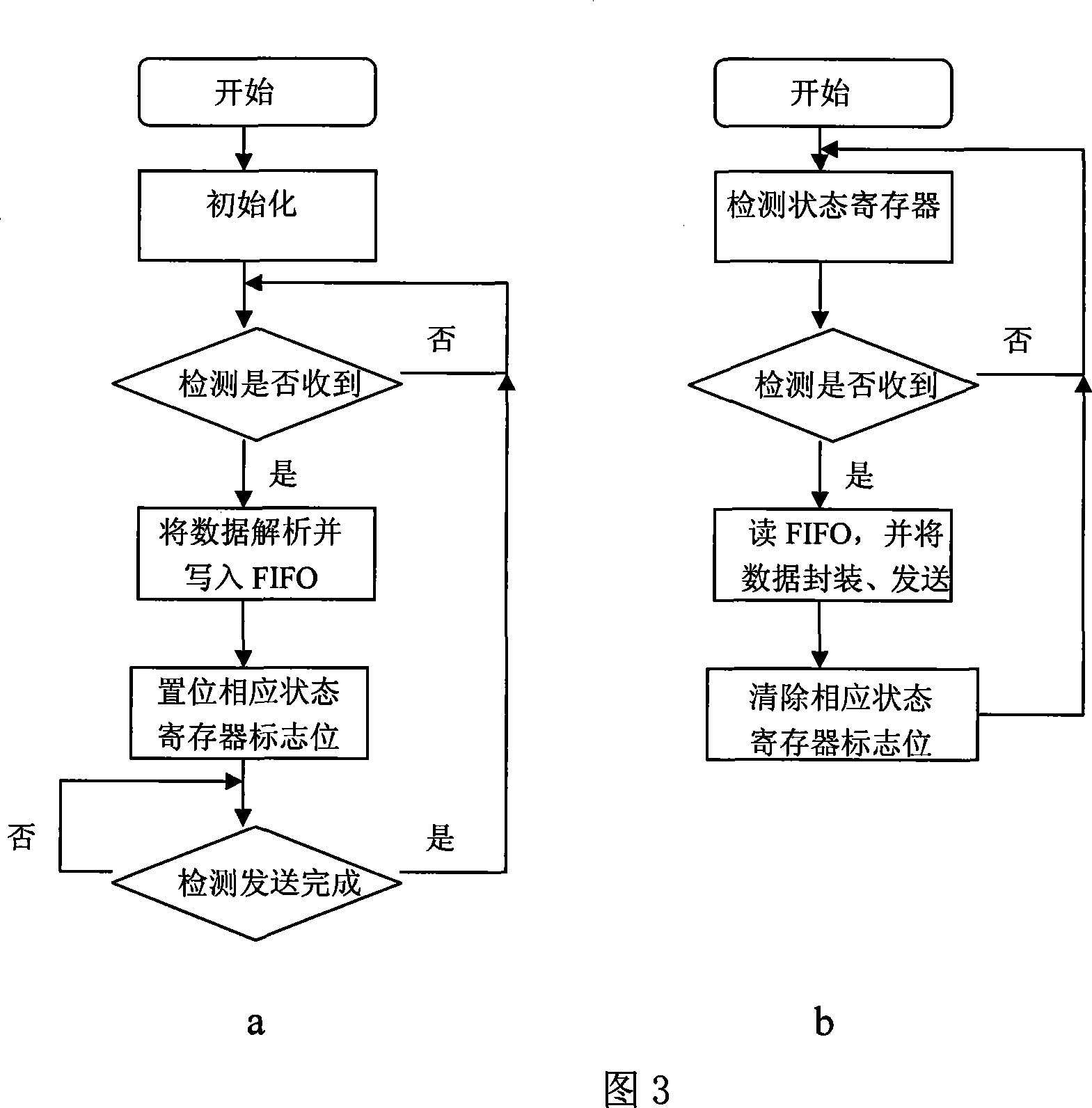
[0025] The present invention will be further described below in conjunction with the accompanying drawings.
[0026] 1. Hardware design
[0027] The hardware structure of the multifunctional communication interface conversion device is shown in Figure 2. The power management module outputs three voltages of 5V, 3.3V and 1.5V. Among them, 5V supplies power to each interface module, while 3.3V and 1.5V supply FPGA. This part of the design only needs to use a general voltage regulator chip to meet the application requirements. The actual 5V power supply uses chip MAX6065, and the 3.3V and 1.5V power supply uses chips ASM1117-3.3 and ASM1117-1.5.
[0028]The FPGA module uses Altera's low-cost chip EP1C6Q240C8, which has a total of 5980 logic units, 185 available IO pins, and a memory of 92160 bits. It uses 1.5V to supply power to the core and 3.3V to supply power to the IO pins. This chip has rich internal resources. , which can fully meet the application requirements of this d...
PUM
 Abstract
Description
Claims
Application Information
 - R&D
- Intellectual Property
- Life Sciences
- Materials
- Tech Scout
- Unparalleled Data Quality
- Higher Quality Content
- 60% Fewer Hallucinations
Browse by: Latest US Patents, China's latest patents, Technical Efficacy Thesaurus, Application Domain, Technology Topic, Popular Technical Reports.
© 2025 PatSnap. All rights reserved.Legal|Privacy policy|Modern Slavery Act Transparency Statement|Sitemap|About US| Contact US: help@patsnap.com


