
Component mounting apparatus and component mounting method

A component assembly and component technology, applied in the field of component assembly devices, can solve the problem of not yet provided component assembly devices, etc., and achieve the effect of high-precision assembly

Active Publication Date: 2007-11-14
PANASONIC CORP
View PDF1 Cites 4 Cited by
  • Summary
  • Abstract
  • Description
  • Claims
  • Application Information

AI Technical Summary

Problems solved by technology

However, there has not been provided a component assembly apparatus that can efficiently perform stack assembly in consideration of the characteristics of this stack assembly

Method used


Image

  • Component mounting apparatus and component mounting method
  • Component mounting apparatus and component mounting method
  • Component mounting apparatus and component mounting method

Examples


no. 1 approach

[0054] Next, embodiments of the present invention will be described in detail with reference to the drawings.

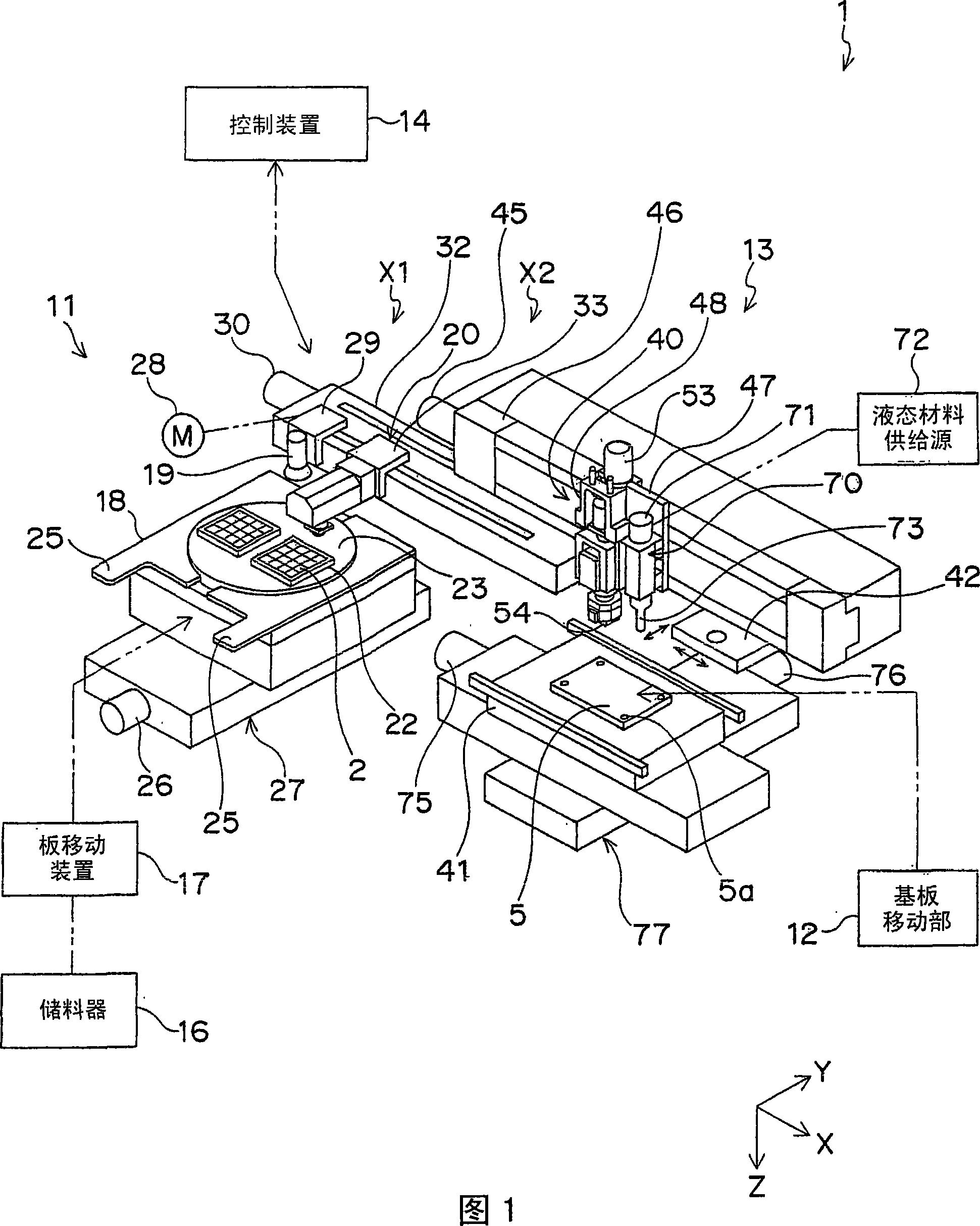
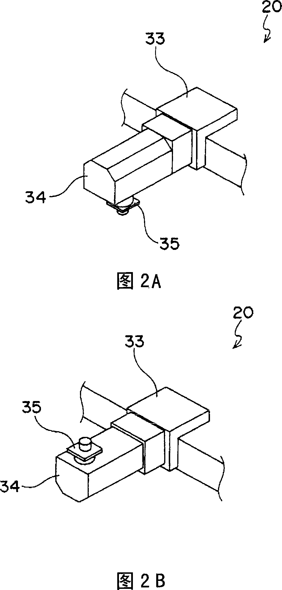
[0055] 1 to 4 show a component mounting apparatus 1 in a first embodiment of the present invention. The component mounting apparatus 1 is an apparatus for stack mounting a plurality of IC chips (components) on a substrate. Referring to Fig. 5A and Fig. 5B, IC chip (hereinafter simply referred to as "chip") 2 is provided with a plurality of pads (such as Au pads) 3 on one side (adsorption surface) 2a, and is provided on the other side (mounting surface 2b) Multiple buffer blocks (eg Au buffer blocks)4. FIG. 6 shows an example of a plurality of chips 2 stacked and mounted on a substrate 5 . As shown in FIG. 6 , a spacer 3 is also provided on the substrate 5 . The chip 2-1 of the first layer is mounted on the substrate 5, and the IC chip 2-2 of the second layer is mounted thereon. In this example, a total of four chips 2-1 to 2-4 are stack-mounted. The bumper 4 of ...

no. 2 approach

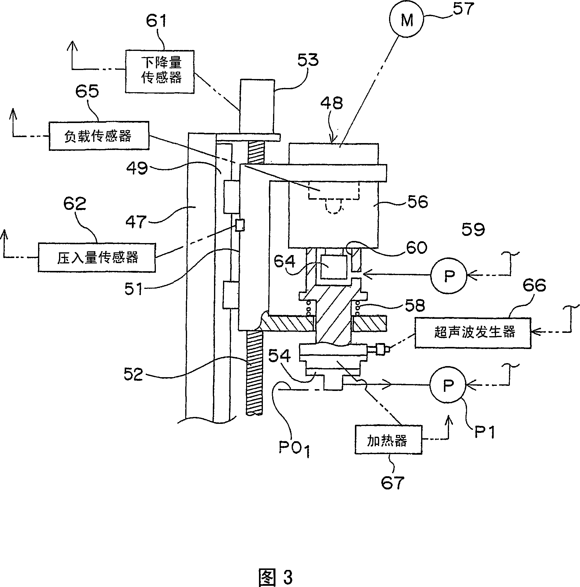
[0117] FIG. 9 shows the control device 14 in the second embodiment of the present invention. In this embodiment, the set pushing amount PHSET of each layer is stored in the data storage unit 101. n . Set the pressing amount PHSET n is a set value as follows, when the mounting head 48 holding the chip 2 on the suction nozzle 54 moves from the first reference height position HB 1 When descending toward the substrate 5 or the mounted chip 2, after the chip 2 held by the suction nozzle 54 contacts the substrate 5 or the mounted chip 2, the assembly head 48 is further lowered, thereby moving the suction nozzle 54 from the initial position P0 1 (Refer to FIG. 3 ) The setting value of the press-fitting distance upward relative to the nozzle support portion 56 in the vertical direction. In addition, the mounting reference height calculating unit 103 sets the set pushing amount PHSET n and the actual pushing amount PHAC detected by the pushing amount sensor 62 as the measured value...

no. 3 approach

[0134] FIG. 12 shows the control device 14 in the third embodiment of the present invention. In this embodiment, the mounting reference height calculation unit 103 uses the actual moving height ZAC as an actual measurement value of the mounting head 48 when the chip 2 is mounted on the substrate 5 or the mounted chip 2 n For assembly reference height H n calculation. The actual moving height ZAC n It is detected by the drop amount sensor 61 . In addition, the actual mobile height ZAC n The datum is the first datum height position HB 1 , and positive downwards in the vertical direction.

[0135] Operations of the control device 14 and the assembly unit 13 will be described with reference to the flowchart of FIG. 13 . In steps S13-1 to S13-12, the processes of steps S13-1, S13-2, S13-4 to S13-9, S13-11, and S13-11 are the same as the processes of the corresponding steps in FIG. 7 . In particular, in step S13-4, the first target moving height calculation unit 104 calculate...


PUM


Abstract

A component mounting apparatus (2) is provided with a stage (41) which has its height position fixed and holds a substrate (5), and a mounting head (48) which releasably holds the chip (2), brings down the chip from a first reference height position (HB1) fixed on an upper part of the stage (41) toward the stage (41), and mounts the chip (2) on the substrate (5) or on the mounted chip (2). A control apparatus (14) is provided with a mounting reference height calculating section (103) for calculating a mounting reference height (Hn) which corresponds to a distance from the first reference height position (HB1), and a first target moving height calculating section (104) for calculating a target moving height (ZTAGn) based on at least the mounting reference height (Hn) and the thickness (PTn) of the chip (2) held by the mounting head (48), and mounts the chip (2) on the substrate (5) or on the mounted chip (2) by bringing down the mounting head (48) from the first reference height position (HB1) to the target moving height (ZTAGn).

Description

technical field [0001] The present invention relates to a component assembly device and a component assembly method. In particular, the present invention relates to a stack assembly device and method for stacking and assembling a plurality of components such as IC chips on a substrate. Background technique [0002] Patent Document 1 discloses a component mounting apparatus for mounting an IC chip on a substrate. The component mounting device is equipped with: a loader (loader) for supplying substrates from the outside of the device; an assembly stage for holding the substrate; a substrate loading device for loading the substrate from the loader onto the assembly stage; Mounting head for mounting IC chips on substrates on the stage; transfer head for transferring IC chips from the component supply unit to the mounting head; unloader for discharging substrates mounted with IC chips from the device to the outside of the device; And a substrate unloading device that unloads a ...

Claims


Application Information

Patent Timeline
Patent Type & Authority Applications(China)
IPC IPC(8): H01L25/065H01L21/60H01L25/07H01L21/52H01L25/18
CPCH01L2924/01006H01L2224/75H01L2924/01004H01L2224/81801H01L24/81H01L2224/81203H01L2224/16H01L2924/01082Y10T29/49131Y10T29/53187Y10T29/53183H01L2924/01084H01L2223/5448H01L2224/81121H01L23/544H01L2224/81205H01L2924/01005H01L2924/01033H01L25/50H01L2924/01047H01L2924/01079H01L2224/759H01L21/67259H01L21/67144H01L2225/06513H01L2924/14H01L2223/54426H01L2924/01078H01L21/563Y10T29/4913Y10T29/49133Y10T29/53178H01L24/75H01L2224/13144Y10T29/53174H01L21/67253Y10T29/53039H01L2224/05573H01L2224/05568H01L2224/05644H01L2924/00014H01L2224/0554H01L2224/05599H01L2224/0555H01L2224/0556H05K13/02H05K13/04
Inventor 平田修一森川诚丸茂伸也上野康晴辻泽孝文
Owner PANASONIC CORP
Learn More