Vacuum plasma reactor used for large area film growth
A plasma and reactor technology, applied in gaseous chemical plating, metal material coating process, coating, etc., can solve the limitation of electrode plate or dielectric plate diameter, unable to make large-area reaction chamber, plasma reaction The device can not meet the use requirements and other problems, so as to avoid leakage, improve uniformity and ensure uniform distribution
- Summary
- Abstract
- Description
- Claims
- Application Information
AI Technical Summary
Problems solved by technology
Method used
Image
Examples
Embodiment 1
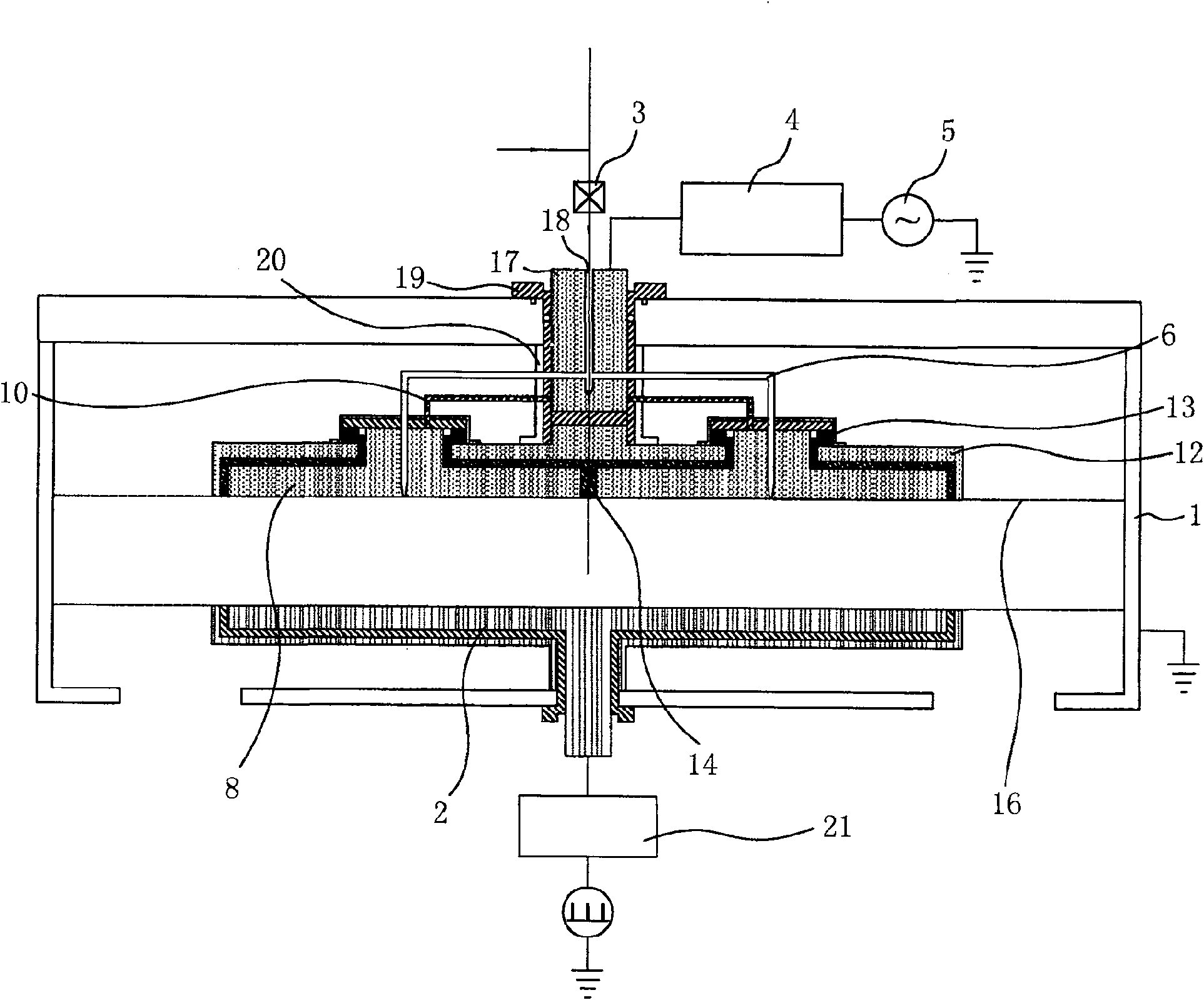
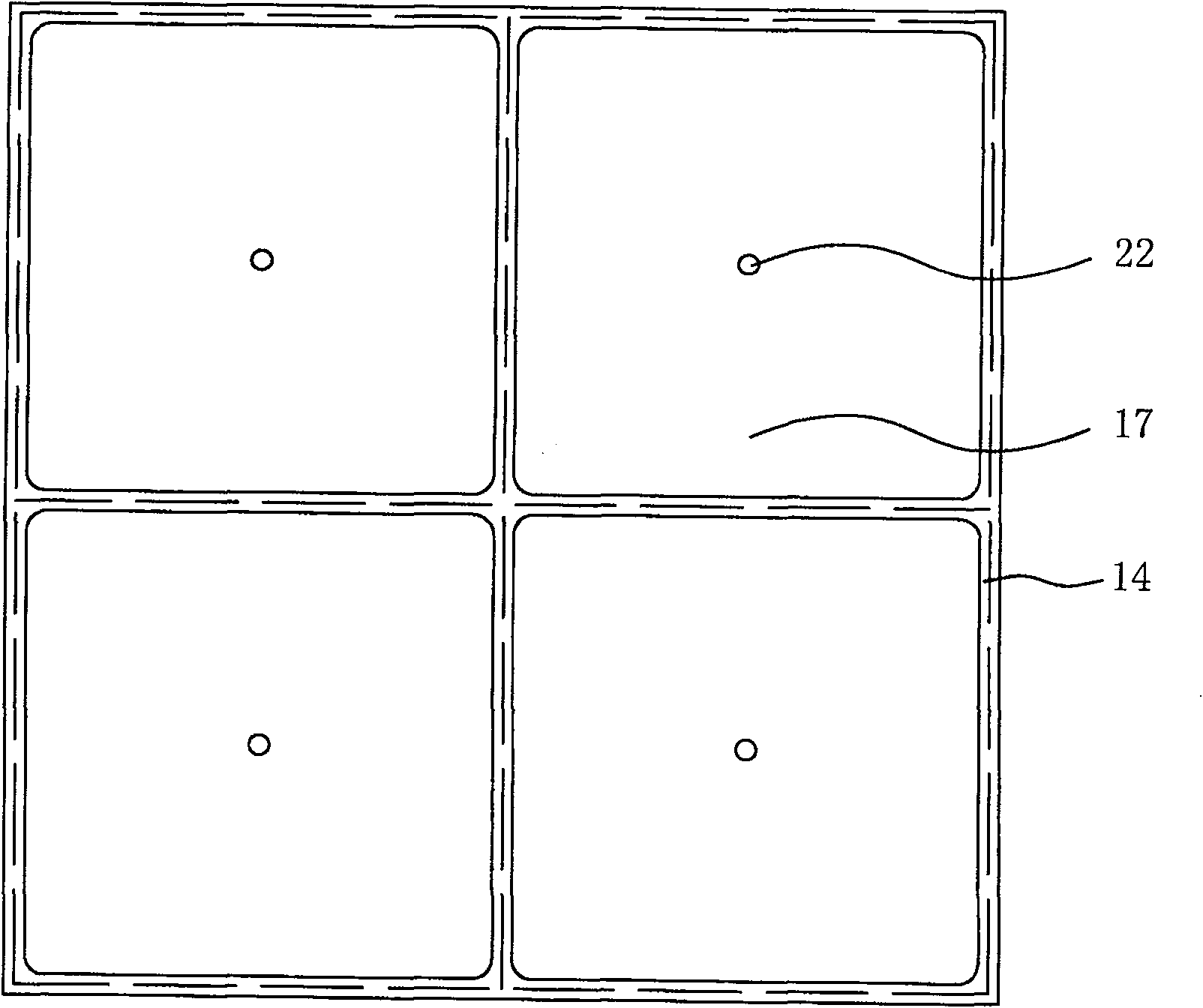
[0026] See attached figure 1 , wherein the plasma reactor includes a vacuum reaction chamber 1, which is preferably configured as a cylindrical design to ensure that the reaction chamber 1 is symmetrical to the axis of symmetry of the entire electrode. The reaction chamber 1 includes a cylindrical highly conductive metal side wall and a top cover, and the bottom of the reaction chamber 1 is two symmetrically placed air inlets, and the reaction chamber 1 is controlled by a vacuum unit (not shown). The interior is vacuumed. A coaxial metal electrode 17 with good electrical conductivity and a coaxial electrical insulating ring 19 are arranged at the axial center of the top cover, and the electrical insulating ring 19 electrically isolates the metal electrode 17 from the top cover. An air inlet 18 is drilled at the center of the metal electrode 17, and is connected to the diversion hole 22 at the center of each electrode plate by the air inlet pipe 6, and is evenly introduced int...
Embodiment 2
[0032] Embodiment 2: The basic structure is the same as that of Embodiment 1. Four groups of square electrode plates (230mm×230mm) are connected in parallel, and the isolation material between them is polytetrafluoroethylene, and the isolation distance is 2 mm. Adjust the vertical position of the substrate holder so that the vertical distance between the substrate holder and the electrode plate is 5 cm. Silane (with H 2 Mixing, mixing ratio is 5: 95) enters in the vacuum chamber 1 with the flow of 150sccm through main gas inlet channel 18 and each minute gas inlet channel 6 and 7, and discharge pressure is 15Pa, and substrate is the glass substrate of large area. A radio frequency power supply with a frequency of 60MHz was started to excite the plasma, the radio frequency power was set to 1200W, and the film deposition time was 30 minutes. The total thickness of the silicon thin film grown on the glass substrate is about 500 nanometers, and the unevenness of the thin film is ...
PUM
| Property | Measurement | Unit |
|---|---|---|
| thickness | aaaaa | aaaaa |
Abstract
Description
Claims
Application Information
 - Generate Ideas
- Intellectual Property
- Life Sciences
- Materials
- Tech Scout
- Unparalleled Data Quality
- Higher Quality Content
- 60% Fewer Hallucinations
Browse by: Latest US Patents, China's latest patents, Technical Efficacy Thesaurus, Application Domain, Technology Topic, Popular Technical Reports.
© 2025 PatSnap. All rights reserved.Legal|Privacy policy|Modern Slavery Act Transparency Statement|Sitemap|About US| Contact US: help@patsnap.com


