Mfg. field emitting vacuum microelectronic element by utilizing nulear track tech and display thereof
A microelectronic device and field emission technology, which is applied in cathode ray lamps/electronic injection lamps, electrical components, image/graphic display tubes, etc., can solve the problems of field emitters without discussion, difficult parameter control, and difficulty in making large sizes, etc. question
- Summary
- Abstract
- Description
- Claims
- Application Information
AI Technical Summary
Problems solved by technology
Method used
Image
Examples
example 1
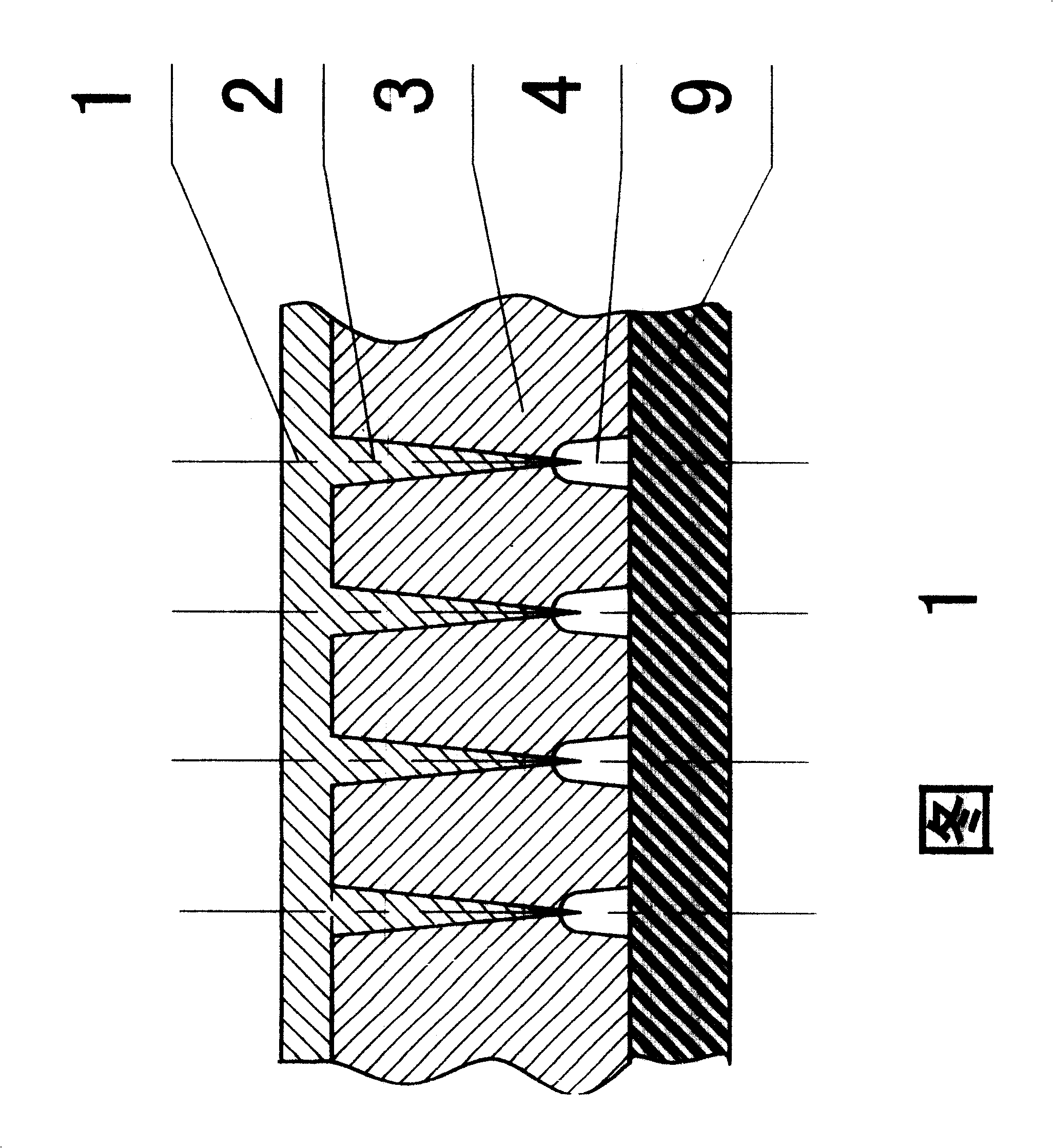
[0098] ①Take a 50 micron thick mica sheet
[0099] ② Utilize uranium ions with a nuclear energy of 7 MeV to vertically irradiate the above-mentioned mica, and the irradiation density is 1×10 7 / cm 2 .
[0100] ③Etch the two sides of the above-mentioned irradiated mica sheet with 40% hydrofluoric acid for different times, so that the etching depth on one side is about 48 microns, and the etching depth on the other side is about 1-2 microns.
[0101] ④ Platinum plating on one side of the etched hole with a depth of 1 to 2 microns
[0102] ⑤ Use the platinum-plated side as the cathode temporarily, fill the mica hole with copper by electrochemical plating until the 48-micron deep cone hole is filled, and plate until the surface is covered to form a base and connections.
[0103] ⑥Remove the temporary platinum layer as the electrode.
[0104] ⑦Use 40% hydrofluoric acid to further etch the 1-2 micron deep hole until the channel hole expands, the tip of the emitter is no longer b...
example 2
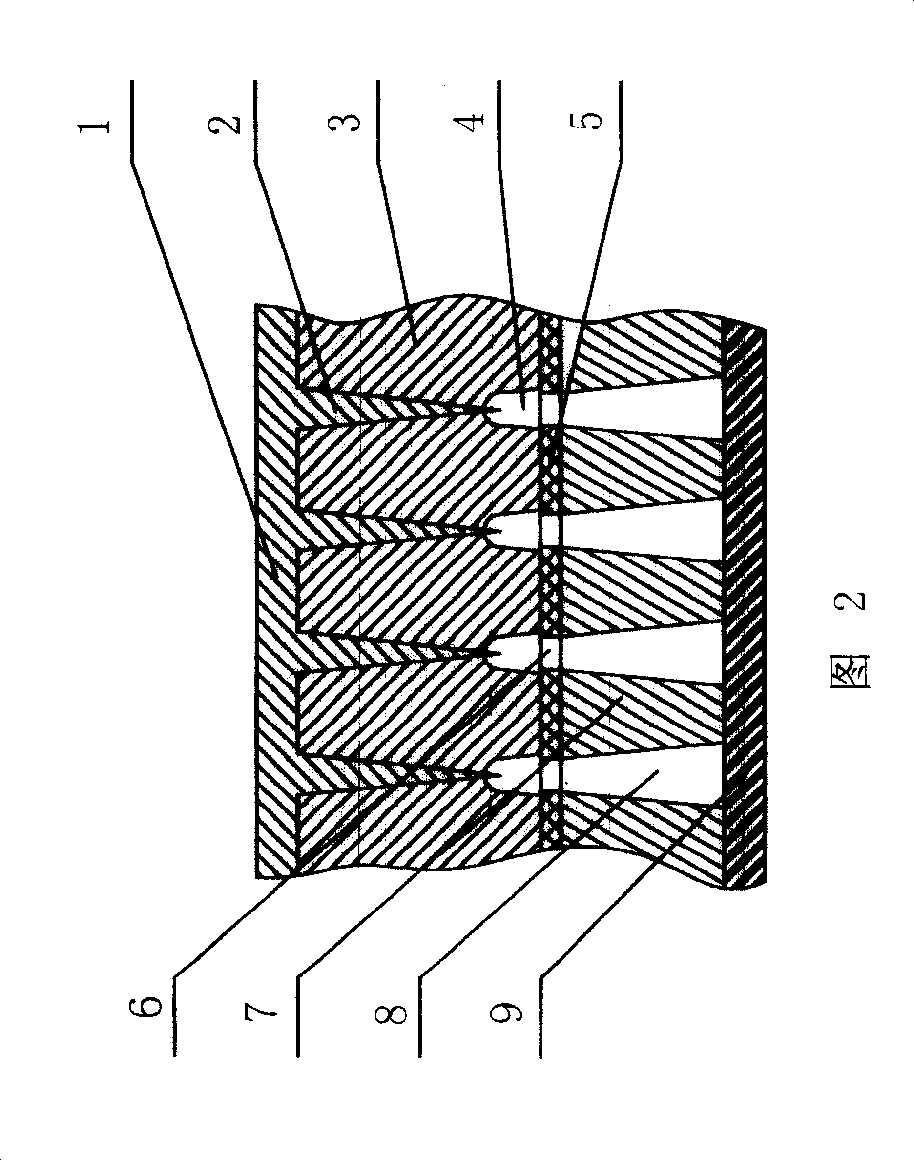
[0106] ① Take a polyester film with a thickness of 4 microns.
[0107] ② Use 20MeV neon ions to irradiate perpendicularly to the above film. Irradiation density 1×10 7 piece / Cm 2 .
[0108] ③ Use 5 mol of sodium hydroxide to perform constant temperature etching on the above-mentioned irradiated polyester film, first measure the track etching rate Vt, and then control the etching time t on both sides of the film 1 =L1 / Vt;t 2 =L2 / Vt. In the formula, L1 is the length of the taper hole on the emitter side, and L2 is the length of the taper hole on the electron channel side.t 1 is t 2 About 3 times of that, the cone hole on the emitter side is about 3 μm deep, and the cone hole on the electron channel side is about 1 μm deep. Or only on the plane where the field emitter is made by t 1 Time etch.
[0109] ④ Plating silver on the field emitter side of the pre-etched thin film by vacuum coating method, so that the deep hole is filled, and a silver layer is formed on the surfac...
example 3
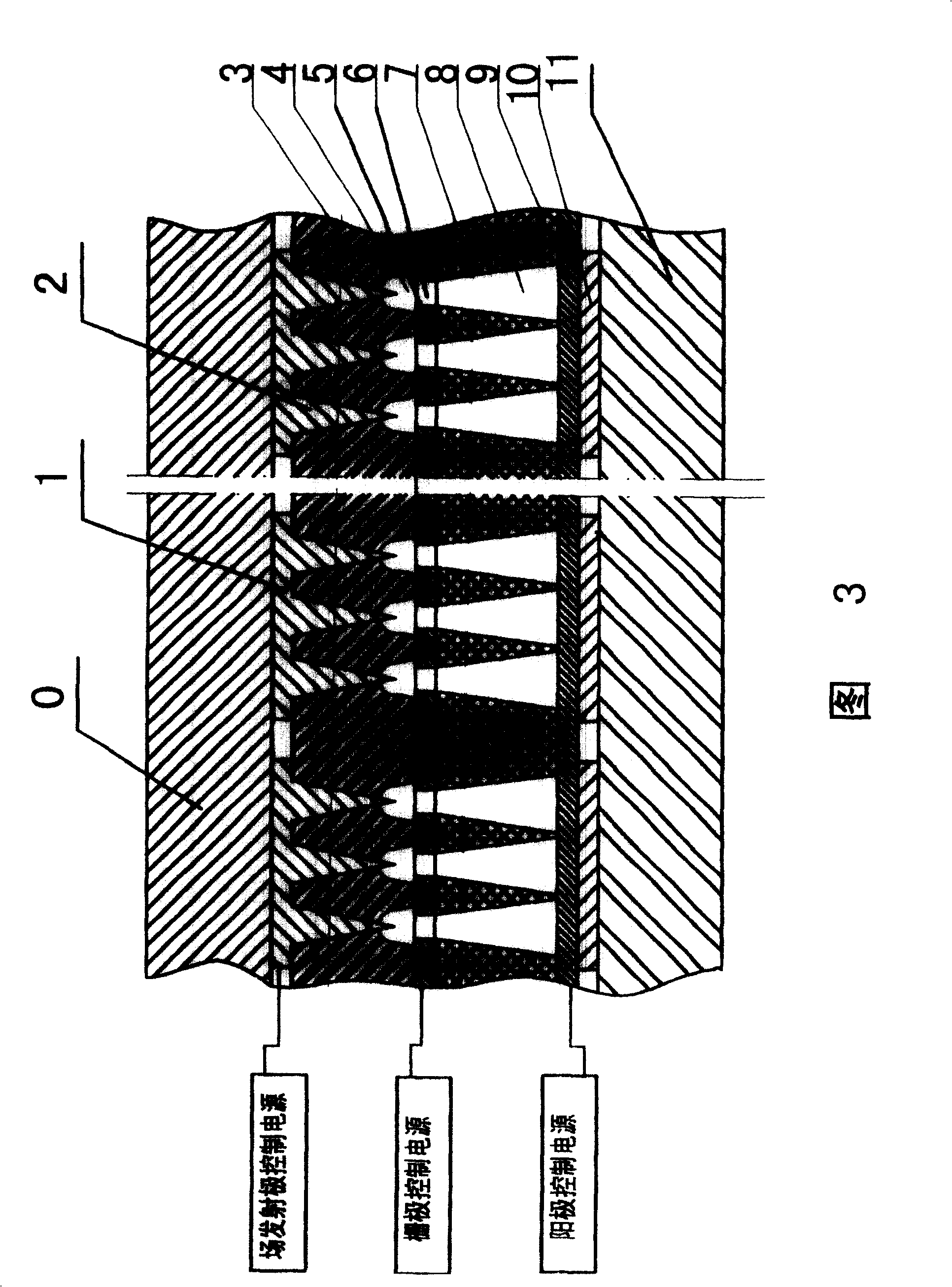
[0112] ①Preparation of polycarbonate-copper-polycarbonate composite material, the thickness of the polycarbonate used as interpolar support A is 4 microns, the thickness of copper is nanoscale, and the thickness of polycarbonate interpolar support B is 8 microns.
[0113] ② Use xenon ions with an energy of 200 Mev to vertically irradiate the above-mentioned composite film with a density of 1×10 8 / cm 2
[0114] ③ Local sensitization treatment is performed on the irradiated composite film by using ultraviolet rays, so that the track etching sensitivity of the substrate A is above 1000.
[0115] ④ Etching the above-mentioned radiation-sensitized composite film with sodium hydroxide solution, the etching time is T=4 / Vt. Make the taper hole on the substrate A reach the copper of the grid, and the diameter of the taper hole is only a few nanometers.
[0116] ⑤ Use the grid as the cathode for the above-mentioned composite film that has been sensitized by radiation and initially e...
PUM
 Abstract
Description
Claims
Application Information
 - Generate Ideas
- Intellectual Property
- Life Sciences
- Materials
- Tech Scout
- Unparalleled Data Quality
- Higher Quality Content
- 60% Fewer Hallucinations
Browse by: Latest US Patents, China's latest patents, Technical Efficacy Thesaurus, Application Domain, Technology Topic, Popular Technical Reports.
© 2025 PatSnap. All rights reserved.Legal|Privacy policy|Modern Slavery Act Transparency Statement|Sitemap|About US| Contact US: help@patsnap.com


