Method of making a microelectronic device

a microelectronic device and microelectronic technology, applied in the direction of cell components, semiconductor/solid-state device details, electric apparatus casings/cabinets/drawers, etc., can solve the problems of the seal and hermeticity of the vias constituted in relation, the vulnerability of the encapsulation solution via a cover, and the rapid degradation of the devi

Active Publication Date: 2017-10-03
COMMISSARIAT A LENERGIE ATOMIQUE ET AUX ENERGIES ALTERNATIVES
View PDF22 Cites 2 Cited by
  • Summary
  • Abstract
  • Description
  • Claims
  • Application Information

AI Technical Summary

Benefits of technology

[0018]As such, the electrical connection for the tapping on a connector operates without calling the seal into question. The sealing seam produces a wall that makes it possible to insulate the electrically conductive material.

Problems solved by technology

The common problem of these circuits and of the active layers that they are comprised of, resides in their rapid degradation in the presence of oxidizing gases of the atmosphere, water and oxygen.
However the problem then arises of the seal and hermeticity of the vias constituted in relation to the oxidizing elements.
In this case, the vulnerability of the encapsulation solutions via a cover depends exclusively on passages created in the cover or in the receiving substrate.

Method used


Image

  • Method of making a microelectronic device
  • Method of making a microelectronic device
  • Method of making a microelectronic device

Examples


Embodiment Construction

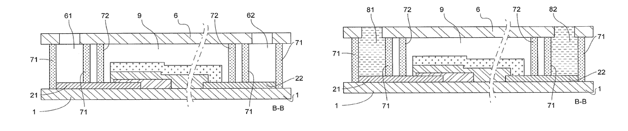
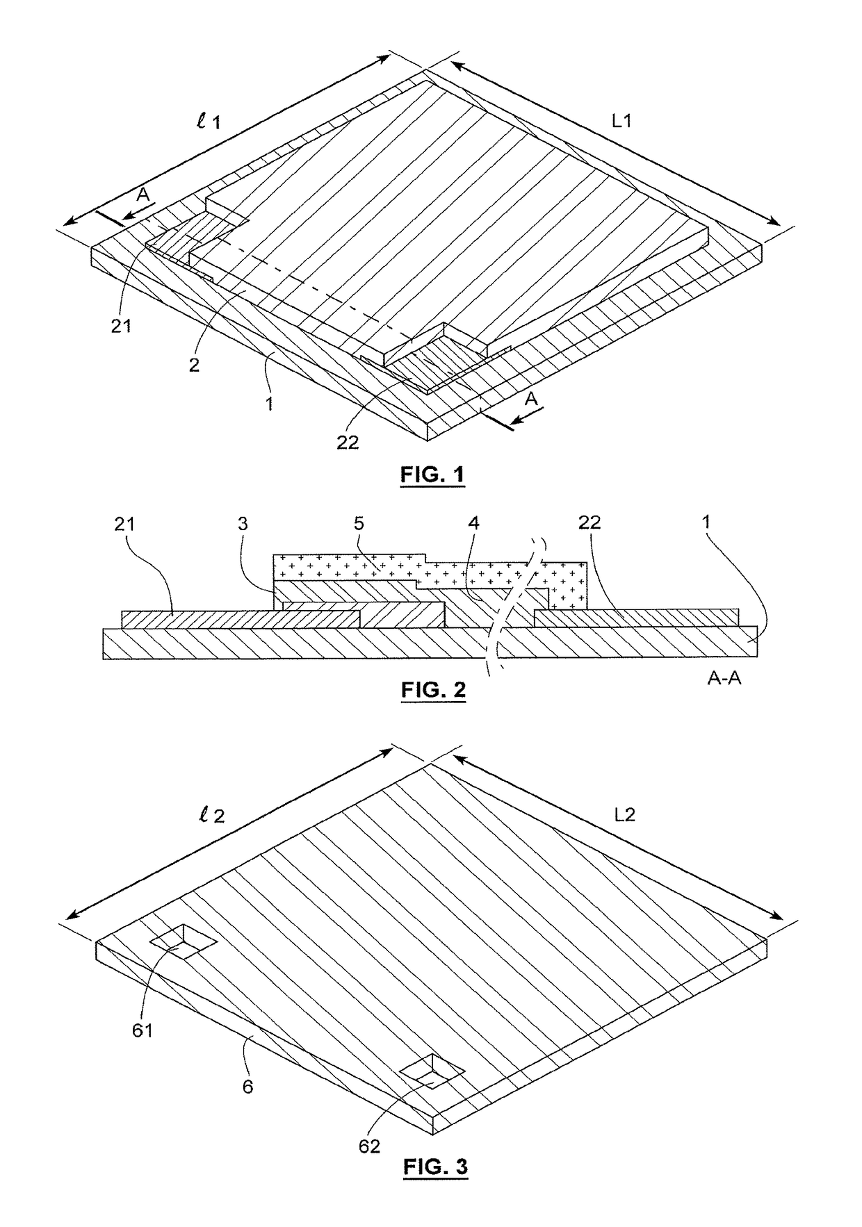
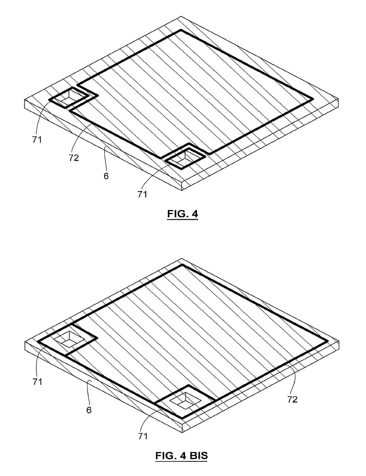
[0032]Before beginning a detailed review of the embodiments of the invention, hereinafter are mentioned the optional characteristics that may be used according to any combination or alternatively:[0033]prior to the step of filling with an electrically conductive material, it is carried out in the support (1) the at least one passage (63, 64) according to a dimension in thickness of said support in such a way that the at least one passage (63, 64) passes through the at least one electrical connector (21, 22);[0034]the step of filling is configured in such a way that the conductive material passes through the support (1) through the at least one passage (63, 64) in such a way as to be exposed on a second face of the support (1), opposite the first face.[0035]the connector (21, 22) is positioned at the periphery of the electronic component (2).[0036]the step of setting in place of the cover (6) is configured to preserve at least one second access to at least one second electrical conne...


PUM

PropertyMeasurementUnit
thicknessaaaaaaaaaa
thicknessaaaaaaaaaa
transformation temperature Tgaaaaaaaaaa

Abstract

This invention relates to a method for producing an electrical system comprising a support (1) bearing on a first face at least one device; with the device comprising at least one electronic component (2) provided with at least one electrical connector (21, 22), with the method comprising: a step of setting in place of a cover (6) positioned above the component; said cover (6) comprising at least one passage (61, 62) according to a dimension in thickness of the cover (6) in such a way as to form an access space to the at least one electrical connector (21, 22), a step of forming a sealing seam (71) in such a way that the component is encapsulated in a sealed cavity (9) delimited by the first face of the support (1), the first face of the cover (6) and the sealing seam (7). The method comprises a step of filling with a conductive material of is at least one passage (61, 62) of the cover (6) in such a way as to establish an electrical continuity between the conductive material and the at least one electrical connector (21, 22), formant a tapping (81, 82) and in that the sealing seam (7) comprises a dielectric material.

Description

FIELD OF THE INVENTION[0001]This invention relates to the encapsulation and the integration of devices in particular microelectronic devices comprising layers that are sensitive to the air. The invention has in particular application in the three-dimensional (3D) assembling of electronic devices with various functionalities (mechanical, optical, optoelectronic, etc.).TECHNOLOGICAL BACKGROUND[0002]In certain applications, in particular in the field of electronics, there is a need to provide circuits with ever-increasing performance, while taking up less and less space. This need tends to be satisfied by providing devices and electronic circuits based on innovative “packaging” architectures, combined with component stacking and assembling technologies and electrical interconnections. The main motivation results from a construction choice of the “packaging” that aims to achieve maximum electrical performance, accompanied by reduced encumbrance.[0003]Generally, thin layer microelectroni...

Claims


Application Information

Patent Timeline
Patent Type & Authority Patents(United States)
IPC IPC(8): H01L21/00H01L51/52H05K3/28H05K1/11H05K5/03H05K5/00H05K3/40H05K1/18H01L31/0203H01M50/103
CPCH05K1/18H01L31/0203H01L51/5253H05K1/115H05K3/284H05K3/4038H05K5/0021H05K5/03H05K2201/20H01L23/04H01L23/10Y02E60/10H01M50/103H10K59/873H10K50/844
Inventor BEDJAOUI, MESSAOUDSALOT, RAPHAEL
Owner COMMISSARIAT A LENERGIE ATOMIQUE ET AUX ENERGIES ALTERNATIVES
Why Eureka
Try Eureka