Pattern dimension measurement method using electron microscope, pattern dimension measurement system, and method for monitoring changes in electron microscope equipment over time
a technology of pattern dimension and measurement method, which is applied in the direction of measuring device, instrument, electric discharge tube, etc., can solve the problem of inevitably affecting the difference between measured values
- Summary
- Abstract
- Description
- Claims
- Application Information
AI Technical Summary
Benefits of technology
Problems solved by technology
Method used
Image

Examples
first embodiment
[ Machine Difference Correction]
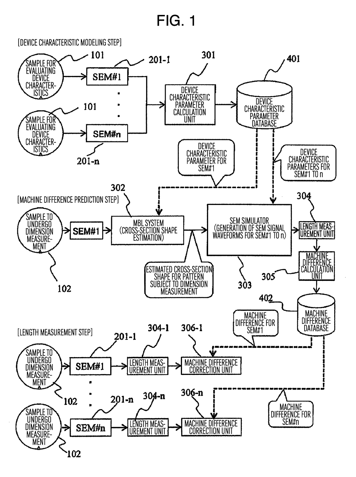
[0062]Referring first to FIG. 1, an overall flow of a pattern dimension measurement corresponding to machine differences according to the present embodiment will be described.
[0063]In the present embodiment, three steps of modeling device characteristics, predicting a machine difference and measuring lengths are provided as necessarily. The respective steps will be described hereinafter.
[Step of Modeling Device Characteristics]
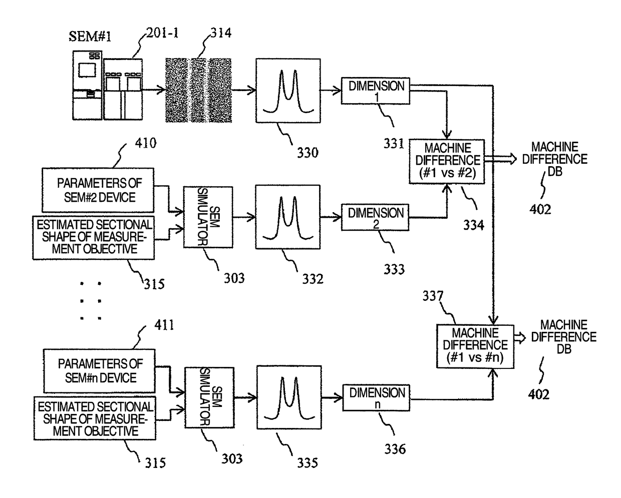
[0064]In the present step, with the use of samples for evaluating device characteristics 101, device characteristic parameters of critical dimension SEM's 201-1 to 201-n are calculated by using a device characteristic parameter calculation unit 301 and the results are stored in a device characteristic parameter database 401.
[0065]Since the present embodiment aims at correcting machine differences, device characteristics having a large impact upon the machine differences are desired to be modeled. In the present embodiment, the d...
second embodiment
[ Monitoring Secular Changes in Device]
[0091]In the first embodiment, the machine difference correction method applied to a plurality of objectives of critical dimension SEM's and the pattern dimension measurement method corresponding to machine differences have been described but the present invention can also be applicable to monitoring secular changes in the respective types of devices. Since details of processing conducted in the second embodiment are similar to those in the processing described in connection with the first embodiment, different points will principally be described hereinafter.
[0092]In order to monitor secular changes in the device, calculation of device characteristic parameters (execution of the step 301 in FIG. 1) is conducted periodically, device parameters are inputted at intervals of a time and SEM signal waveforms are generated (execution of the steps 303 and 304 in FIG. 1). In this phase, the device characteristic parameters periodically calculated are s...
PUM
 Abstract
Description
Claims
Application Information
 - R&D Engineer
- R&D Manager
- IP Professional
- Industry Leading Data Capabilities
- Powerful AI technology
- Patent DNA Extraction
Browse by: Latest US Patents, China's latest patents, Technical Efficacy Thesaurus, Application Domain, Technology Topic.
© 2024 PatSnap. All rights reserved.Legal|Privacy policy|Modern Slavery Act Transparency Statement|Sitemap