Slow wave RF propagation line including a network of nanowires
a nanowire and propagation line technology, applied in delay lines, waveguides, electrical equipment, etc., can solve the problems of low loss, large surface area, and disadvantage of occupying a relatively large area, and achieve the effect of low loss
- Summary
- Abstract
- Description
- Claims
- Application Information
AI Technical Summary
Benefits of technology
Problems solved by technology
Method used
Image
Examples
Embodiment Construction
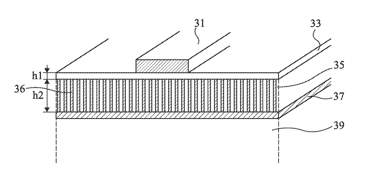
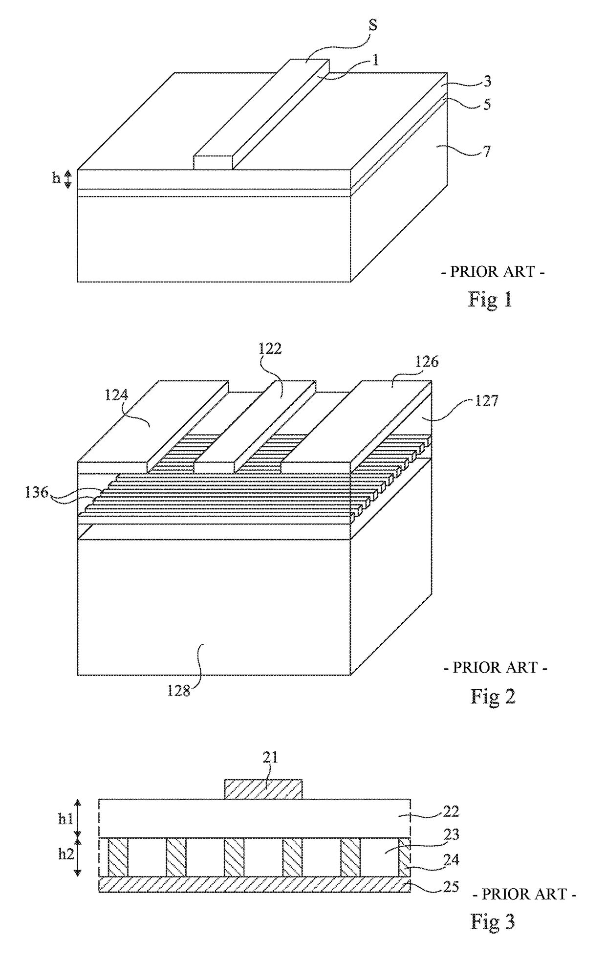
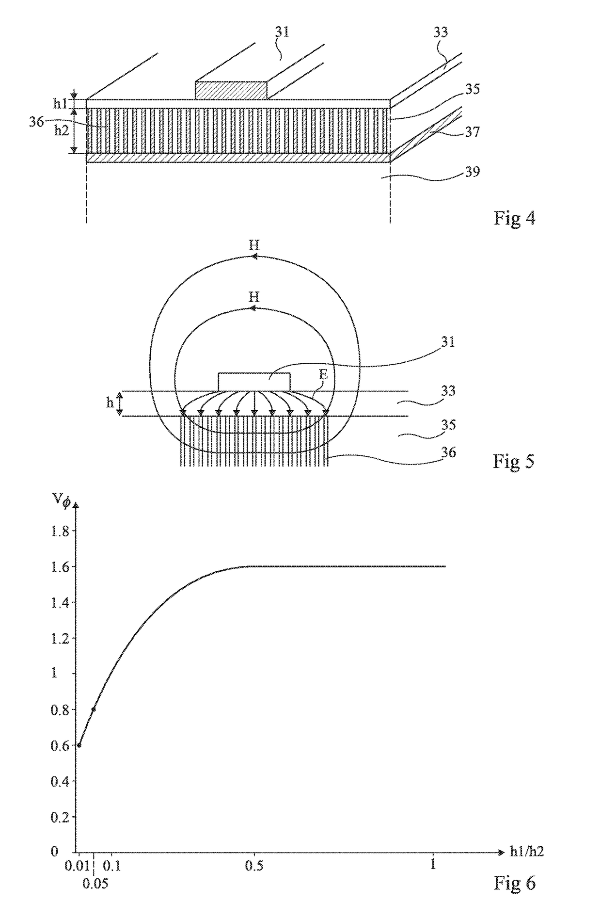
[0029]FIG. 4 shows an embodiment of a microstrip-type line. A conductive strip 31 is laid on a first insulating layer 33 having a thickness h1, formed on a second insulating layer 35 laid on a ground plane 37 which may be formed above a substrate 39. Insulating layer 33 may be a layer of silicon oxide or of another insulating material currently used in integrated circuit manufacturing. Layer 37 for example has a thickness from 0.5 to 2 μm. Second insulating layer 35 for example is a layer of a ceramic such as alumina. Layer 35 is provided with substantially vertical cavities (in a plane orthogonal to the plane of strip line 31). The cavities are filled with nanowires 36 made of a non-magnetic conductive material, for example, copper, aluminum, silver, or gold, in electric contact with ground plane 37. Various ways to manufacture a nanowire network in an alumina membrane of variable porosity are known and may be used. According to an advantage, nanowires 36 may have a small diameter,...
PUM
 Abstract
Description
Claims
Application Information
 - R&D
- Intellectual Property
- Life Sciences
- Materials
- Tech Scout
- Unparalleled Data Quality
- Higher Quality Content
- 60% Fewer Hallucinations
Browse by: Latest US Patents, China's latest patents, Technical Efficacy Thesaurus, Application Domain, Technology Topic, Popular Technical Reports.
© 2025 PatSnap. All rights reserved.Legal|Privacy policy|Modern Slavery Act Transparency Statement|Sitemap|About US| Contact US: help@patsnap.com


