AMOLED backplane structure and manufacturing method thereof
a backplane and amoled technology, applied in the field of amoled backplane structure, can solve the problems of reducing resolution, accelerating aging of oled materials, design difficulty, etc., and achieve the effects of ensuring smoothness of a planarization layer, increasing the effective displaying area, and prolonging the life of an oled
- Summary
- Abstract
- Description
- Claims
- Application Information
AI Technical Summary
Benefits of technology
Problems solved by technology
Method used
Image
Examples
first embodiment
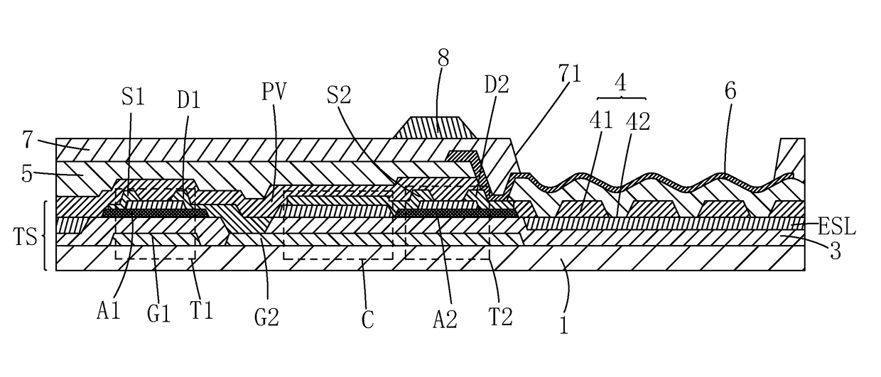
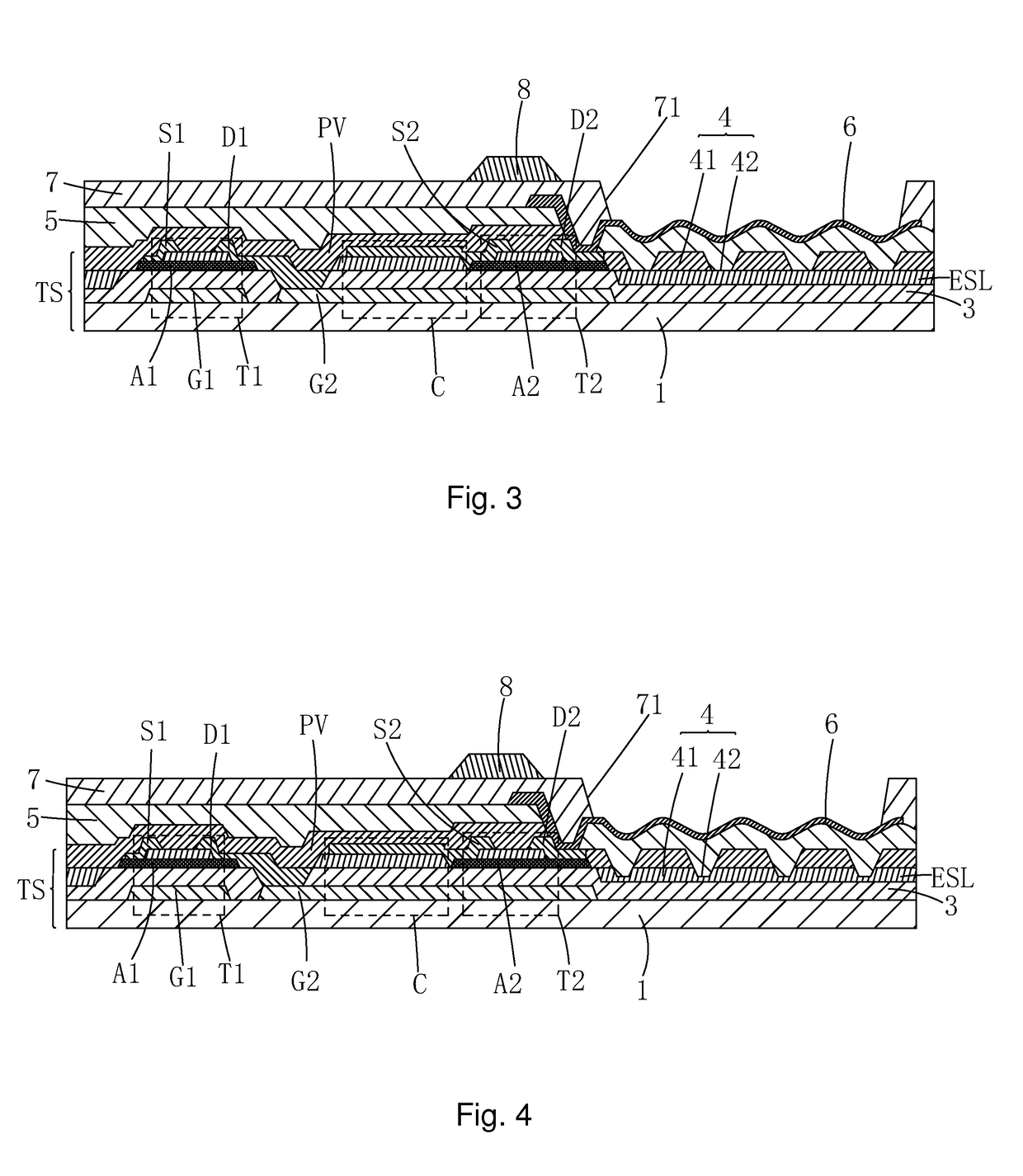
[0052]Firstly, the present invent provides an AMOLED backplane structure. Referring to FIG. 3, an AMOLED backplane structure according to the present invention is shown, which comprises multiple sub-pixels arranged in an array. In each of the sub-pixels, the AMOLED backplane comprises: a thin-film transistor (TFT) substrate TS, a planarization layer 5 formed on the TFT substrate TS, a pixel electrode 6 formed on the planarization layer 5, a pixel definition layer 7 formed on the pixel electrode 6, and a photo spacer 8 formed on the pixel definition layer 7.
[0053]The TFT substrate TS comprises therein a switch TFT T1, a drive TFT T2, and a capacitor C.
[0054]The pixel definition layer 7 comprises an opening 71 formed therein to expose a portion of the pixel electrode 6.
[0055]The TFT substrate TS comprises a corrugation structure 4 arranged in an area corresponding to the opening 71 of the pixel definition layer 7. The corrugation structure 4 comprises a plurality of raised sections 41...
second embodiment
[0066]For the AMOLED backplane structure of the second embodiment shown in FIG. 4, in Step 1, in the same time of forming a protective layer PV, the protective layer PV and an etch stop layer ESL are both subjected to dry etching to form the corrugation structure 4.
third embodiment
[0067]For the AMOLED backplane structure of the third embodiment shown in FIG. 5, in Step 1, in the same time of forming first source and drain terminals S1, D1 and second source and drain terminals S2, D2, a metal layer M is subjected to dry etching to form the corrugation structure 4.
[0068]Step 2: as shown in FIG. 6, with the AMOLED backplane structure of the first embodiment shown in FIG. 3 being taken as an example, coating organic photoresist on the TFT substrate TS that comprises the corrugation structure 4 formed thereon to form a planarization layer 5 in such a way that an upper surface of a portion of the planarization layer 5 corresponding to and located above the corrugation structure 4 comprises a curved configuration corresponding to the corrugation structure 4 in order to ensure smoothness of the planarization layer and thus being free of abrupt change site.
[0069]In Step 2, the organic photoresist is directly coated to form the planarization layer 5 without a gray scal...
PUM
 Abstract
Description
Claims
Application Information
 - R&D
- Intellectual Property
- Life Sciences
- Materials
- Tech Scout
- Unparalleled Data Quality
- Higher Quality Content
- 60% Fewer Hallucinations
Browse by: Latest US Patents, China's latest patents, Technical Efficacy Thesaurus, Application Domain, Technology Topic, Popular Technical Reports.
© 2025 PatSnap. All rights reserved.Legal|Privacy policy|Modern Slavery Act Transparency Statement|Sitemap|About US| Contact US: help@patsnap.com


