In-plane switching mode liquid crystal display device and fabrication method thereof

a liquid crystal display and switching mode technology, applied in the field of liquid crystal display devices, can solve the problems of serious deterioration in display performance, which has not yet been applied in mass production, and achieves the effects of improving display visibility, simple process, and low pretilt angl

Active Publication Date: 2017-02-28
PUSAN NAT UNIV IND UNIV COOPERATION FOUND
View PDF9 Cites 0 Cited by
  • Summary
  • Abstract
  • Description
  • Claims
  • Application Information

AI Technical Summary

Benefits of technology

[0042]Firstly, it is possible to obtain a low pretilt angle by a simple process without deterioration in other electro-optic characteristics and thus possible to greatly improve visibility for display.
[0043]Secondly, it is possible to improve performance without a great change in a process by performing a UV process while a vertical voltage / electric field is applied to an alignment agent in which a photocurable polymer is mixed.
[0044]Thirdly, it is possible to realize a high surface anchoring energy, a low UV curing energy, and a simple process by a conventional rubbing process without a great change in a process.

Problems solved by technology

A light leakage caused by a pretilt angle cannot be improved by viewing angle compensation using a compensation film and thus causes a serious deterioration in performance of a display.
As one of the studies, a study of photo alignment using strong UV rays has been conducted, but has not yet been applied to mass production due to many disadvantages.

Method used


Image

  • In-plane switching mode liquid crystal display device and fabrication method thereof
  • In-plane switching mode liquid crystal display device and fabrication method thereof
  • In-plane switching mode liquid crystal display device and fabrication method thereof

Examples


Embodiment Construction

[0053]Exemplary embodiments of an in-plane switching mode liquid crystal display device and a fabrication method thereof according to the present invention will now be described in detail with reference to the accompanying drawings.

[0054]Features and advantages of the in-plane switching mode liquid crystal display device and the fabrication method thereof according to the present invention will be apparent from the following detailed descriptions of each exemplary embodiment.

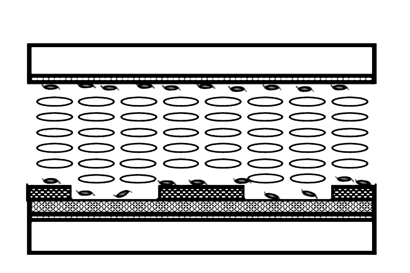
[0055]FIG. 3 is a configuration view illustrating a cross section of a three-electrode in-plane switching mode liquid crystal cell according to an exemplary embodiment of the present invention, and FIGS. 4a through 4d are cross-sectional views of a fabrication process including liquid crystal alignment using a rubbing process so as to have a low pretilt angle.

[0056]The present invention is provided to improve visibility without deterioration in other electro-optic characteristics by applying a three-electrode st...


PUM

PropertyMeasurementUnit
pretilt angleaaaaaaaaaa

Abstract

There are provided an in-plane switching mode liquid crystal display device and a fabrication method of the in-plane switching mode liquid crystal display device which has a low pretilt angle by applying a three-electrode structure to an in-plane switching display and mixing a photocurable polymer into an alignment film by a rubbing process, and includes: an upper substrate having an upper plate conductive electrode; a lower substrate having a lower plate conductive electrode and a pattern electrode formed on the lower plate conductive electrode with an insulating layer therebetween; the liquid crystal layer disposed between the upper substrate and the lower substrate; and an alignment film formed on the upper substrate having the upper plate conductive electrode and the lower substrate having the pattern electrode and configured to align liquid crystals in an in-plane manner.

Description

CROSS-REFERENCE TO RELATED APPLICATIONS[0001]This application claims the priority of Korean Patent[0002]Application No. 10-2014-0176176 filed on Dec. 9, 2014, in the Korean Intellectual Property Office, the disclosure of which is incorporated herein by reference.BACKGROUND OF THE INVENTION[0003]Field of the Invention[0004]The present invention relates to a liquid crystal display device, and more particularly, to an in-plane switching mode liquid crystal display device and a fabrication method of the in-plane switching mode liquid crystal display device which has a low pretilt angle by applying a three-electrode structure to an in-plane switching display and mixing a photocurable polymer into an alignment film by a rubbing process.[0005]Description of the Related Art[0006]A liquid crystal display device is one of flat panel display devices and configured to control an amount of light to be transmitted by applying a voltage to an electrode and rearranging liquid crystal molecules in a...

Claims


Application Information

Patent Timeline
Patent Type & Authority Patents(United States)
IPC IPC(8): G02F1/1337G02F1/1343
CPCG02F1/134363G02F1/133784G02F1/133788G02F2001/133738G02F2001/133749G02F1/133738G02F1/133749G02F1/1337G02F1/133711G02F1/133753G02F1/134309
Inventor YOON, TAEHOONOH, SEUNGWONPARK, JUNHEE
Owner PUSAN NAT UNIV IND UNIV COOPERATION FOUND
Why Eureka
Try Eureka