Image sensor, production method therefor, and inspection apparatus
a technology of image sensor and production method, applied in the field of image sensor, can solve the problems of limited detection efficiency, and achieve the effect of reducing crosstalk between pixels and improving light collection efficiency
- Summary
- Abstract
- Description
- Claims
- Application Information
AI Technical Summary
Benefits of technology
Problems solved by technology
Method used
Image
Examples
second embodiment
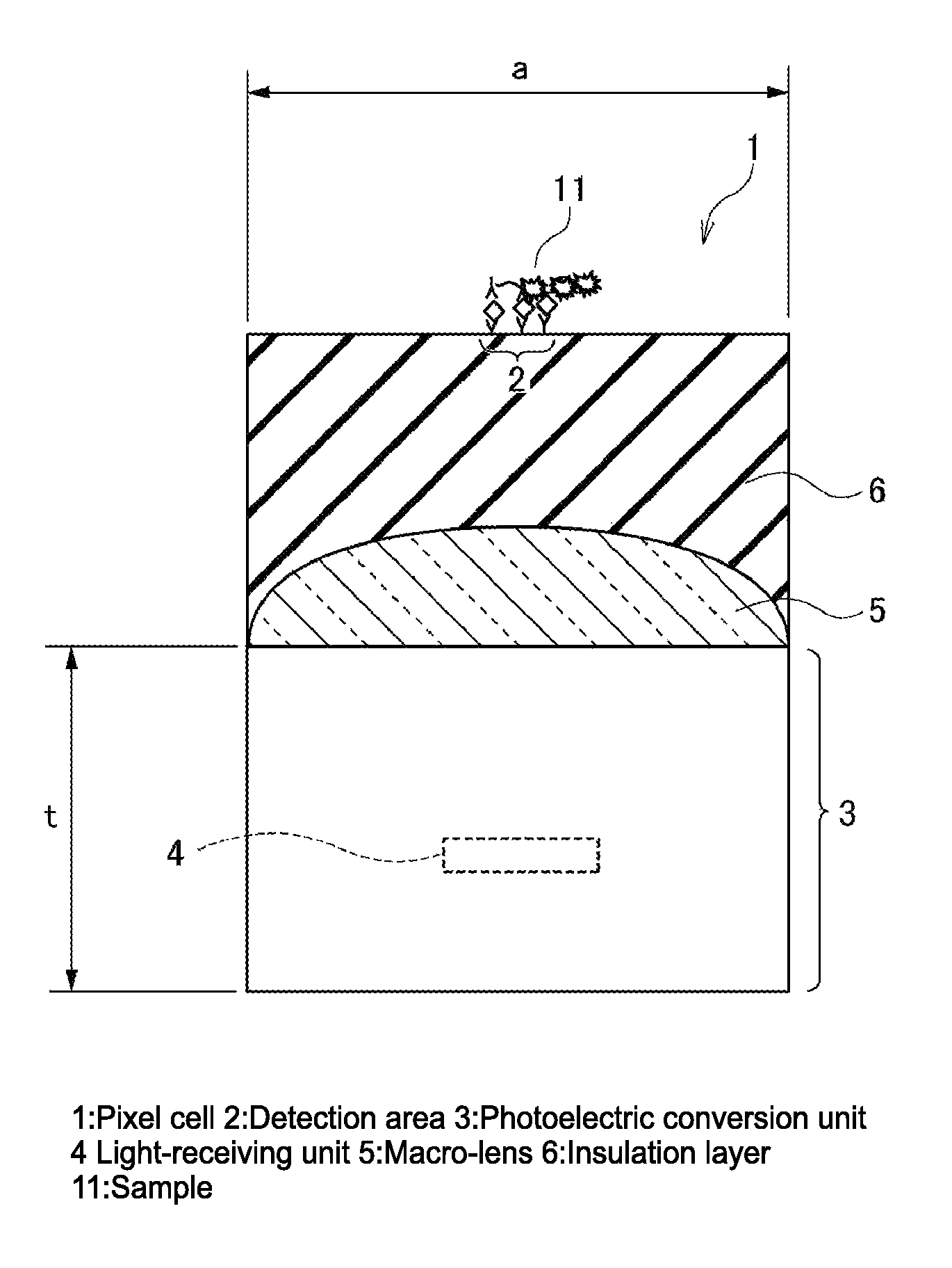
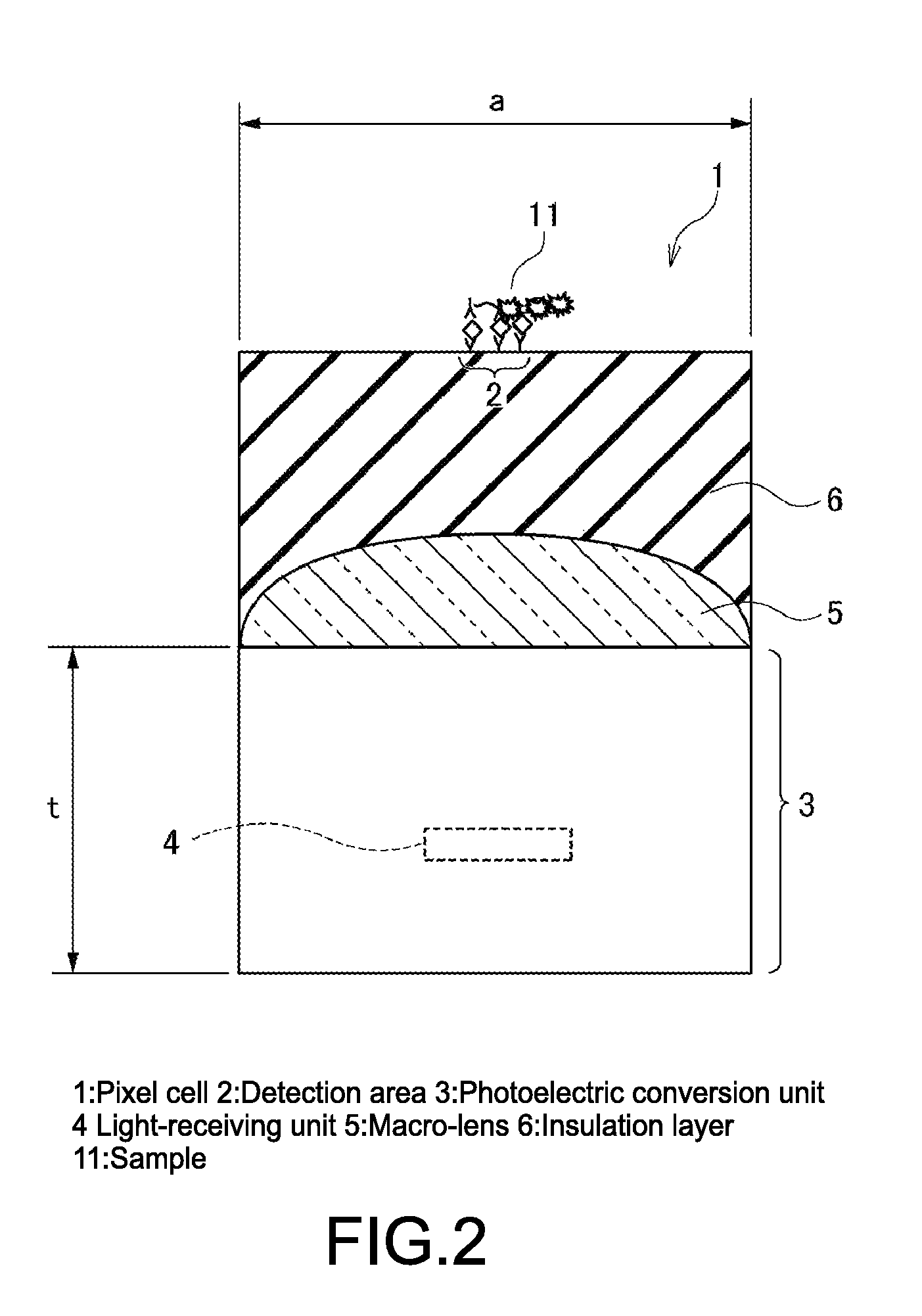
[0073]Next, an image sensor according to a second embodiment of the present disclosure will be described. FIG. 8 is a cross-sectional diagram showing a structure of a pixel cell of the image sensor of this embodiment. It should be noted that in FIG. 8, constituent elements that are the same as those of the pixel cell 1 of the image sensor according to the first embodiment shown in FIG. 2 are denoted by the same symbols, and detailed descriptions thereof will be omitted.
(Overall Structure)
[0074]As shown in FIG. 8, in the image sensor of this embodiment, a light shield mask 22 that shields light is formed in a portion excluding the detection area 2 on the surface of the insulation layer 6.
(Light Shield Mask 22)
[0075]The material of the light shield mask 22 is not particularly limited as long as it absorbs and / or reflects light such as the excitation light 12 and the fluorescent light 13 emitted from the sample 11, but can be formed using, for example, an aluminum thin film, a chrome o...
third embodiment
[0078]Next, an inspection apparatus according to a third embodiment of the present disclosure will be described. FIG. 9 is a block diagram showing a structure of the inspection apparatus of this embodiment. As shown in FIG. 9, the image sensor 10 according to the first embodiment described above is mounted on the inspection apparatus 30 of this embodiment, and by irradiating light emitted from a light source 32 onto a sample 11 injected from a sample injection unit 33, for example, a luminescence process thereof is detected.
[0079]An image pickup apparatus 31 of the inspection apparatus 30 includes, in addition to the image sensor 10, an image processing unit 34 that processes a detection signal, a memory 35 that stores processed data, a display unit 36 as a display, and a transmission unit 37 that transmits data in the memory 35. The image pickup apparatus 31 also includes a controller 38 that controls the image sensor 10, the image processing unit 34, the transmission unit 37, the ...
PUM
| Property | Measurement | Unit |
|---|---|---|
| thickness | aaaaa | aaaaa |
| refractive index | aaaaa | aaaaa |
| thickness | aaaaa | aaaaa |
Abstract
Description
Claims
Application Information
 - R&D
- Intellectual Property
- Life Sciences
- Materials
- Tech Scout
- Unparalleled Data Quality
- Higher Quality Content
- 60% Fewer Hallucinations
Browse by: Latest US Patents, China's latest patents, Technical Efficacy Thesaurus, Application Domain, Technology Topic, Popular Technical Reports.
© 2025 PatSnap. All rights reserved.Legal|Privacy policy|Modern Slavery Act Transparency Statement|Sitemap|About US| Contact US: help@patsnap.com


