Method and device for active load modulation by inductive coupling

a technology of active load and inductive coupling, which is applied in the direction of synchronisation signal speed/phase control, near-field system using receivers, instruments, etc., can solve the problems of high cost, unsatisfactory fluctuations in communication distance, and high precision requirements

Active Publication Date: 2014-09-16
VERIMATRIX INC
View PDF27 Cites 7 Cited by
  • Summary
  • Abstract
  • Description
  • Claims
  • Application Information

AI Technical Summary

Benefits of technology

The present invention proposes a method and device for transmitting data using an inductive antenna circuit. The method involves using a synchronous oscillator and resynchronizing it with an external magnetic field before each application of a burst of a periodic signal to the antenna circuit. The device includes an inductive antenna circuit, a synchronous oscillator, and an active load modulation circuit. The device can generate or receive a data carrying load modulation signal and apply it to the antenna circuit when the modulation signal has a first logic value. The method and device can be used in a data emission / reception device and can be mounted in or on a portable support or chip card. The technical effects of the invention include improved data transmission accuracy and stability, as well as improved device portability and reliability.

Problems solved by technology

Phase rotations between the active load modulation magnetic field and the external magnetic field may cause undesirable fluctuations in the communication distance.
Such a precision requires a very high quality and expensive circuitry.

Method used


Image

  • Method and device for active load modulation by inductive coupling
  • Method and device for active load modulation by inductive coupling
  • Method and device for active load modulation by inductive coupling

Examples


Embodiment Construction

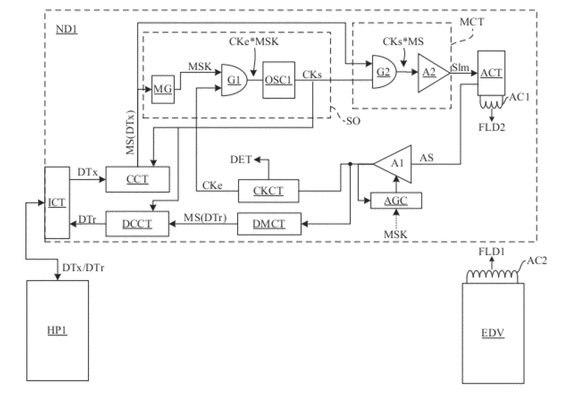
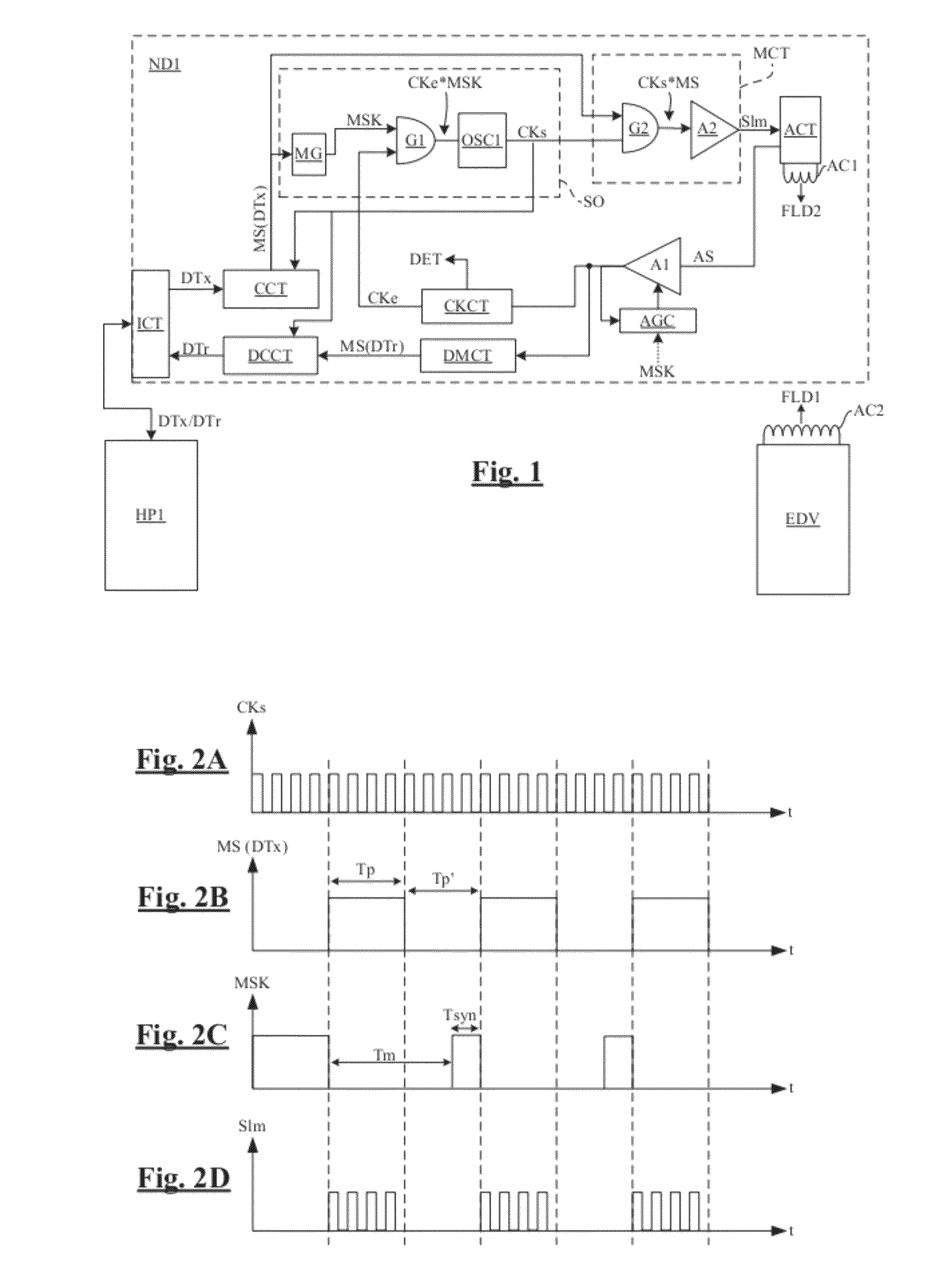
[0046]FIG. 1 shows a data emission / reception device ND1 according to an embodiment of the invention, functioning by inductive coupling. Device ND1 includes:[0047]a contact communication interface circuit ICT,[0048]an antenna circuit ACT turned to a carrier frequency, including an antenna coil AC1 and may optionally include various other components such as capacitors and / or inductors,[0049]a demodulation circuit DMCT coupled to a decoding circuit DCCT, to receive data DTr via the antenna circuit,[0050]a coding circuit CCT coupled to a modulation circuit MCT, to transmit data DTx via the antenna circuit,[0051]a clock circuit CKCT, and[0052]a synchronous oscillator SO.

[0053]Contact communication interface circuit ICT allows device ND1 to be linked to at least one host processor HP1. Host processor HP1 supplies data DTx and receives data DTr. Data DTx / DTr are generally application data of an NFC application NFC (transaction, payment, exchange of information, etc.). In one variation, dev...


PUM


Abstract

A data emission / reception device by inductive coupling includes an inductive antenna circuit in which an antenna signal appears, a mechanism configured to for extracting a first periodic signal from the antenna signal, a synchronous oscillator receiving the first periodic signal and supplying a second periodic signal, and an active load modulation circuit configured to apply bursts of the second periodic signal to the antenna circuit. The device is configured to place the oscillator in the synchronous oscillation mode before each application of a burst of the second periodic signal to the antenna circuit, then place the oscillator in the free oscillation mode.

Description

BACKGROUND OF THE INVENTION[0001]Embodiments of the present invention relate to a method of transmitting data by inductive coupling, including the steps of receiving an antenna signal using an inductive antenna circuit in the presence of an alternating external magnetic field, extracting from the antenna signal a first periodic signal, producing a second periodic signal using a synchronous oscillator having a synchronization input receiving the first periodic signal, placing the oscillator in a free oscillation mode, and applying to the antenna circuit bursts of the second periodic signal to generate an active load modulation magnetic field.[0002]Embodiments of the present invention also relate to a device for transmitting and receiving data configured to implement this method.[0003]In a general manner, embodiments of the present invention relate to inductive coupling communication techniques, also known as “Near Field Communications” or NFC. A communication by inductive coupling ge...

Claims


Application Information

Patent Timeline
Patent Type & Authority Patents(United States)
IPC IPC(8): H04B5/00G06K19/07
CPCH04B5/0031G06K19/0723H04B5/72H04B5/00H04L27/00H04B5/48H04B1/3816H04L7/08
Inventor CHARRAT, BRUNOPERNISEK, FLORIAN
Owner VERIMATRIX INC
Why Eureka
Try Eureka