
Apparatus and method for optimized power cell synthesizer

a power cell and synthesizer technology, applied in the field of design of ics, can solve the problems of cumbersome comprehensive optimization look-up table, inability to achieve satisfactory results, and increasing the size of ics

Active Publication Date: 2014-06-24
GLOBALFOUNDRIES U S INC
View PDF12 Cites 4 Cited by
  • Summary
  • Abstract
  • Description
  • Claims
  • Application Information

AI Technical Summary

Problems solved by technology

Clearly, increasing gate width comes at the expense of increased area consumed by a power transistor in an IC, ultimately increasing the size of the IC.
When the goal is to minimize RDSon, this circumstance leads to striking a balance between Rint and Rmetal, a non-monotonic problem.
However, previously, multivariate nonlinear optimization of parameters, intending to produce a target value for a predetermined figure of merit, has been avoided in favor of more simplistic “tweaks,” which may involve numerous iterations from design through fabrication, and which still may not achieve a satisfactory outcome.
While an impressive feat, such data sets tend to use significant economic, personnel, training, and infrastructure resources to develop, to maintain, and to update and adapt.
A comprehensive optimization look-up table also tends to be cumbersome and inherently inertial, reducing a design team's ability to meet the rapidly changing requirements and short product cycles.
As the number of parameters and ranges of parameters in dimension and scope, there is a greater likelihood of a quantization error-type of imprecision of the data, which lead away from the global minimum.
Overall, these methodologies contain shortcomings that can lead to overdesign, increased costs, and longer design times. In an example of overdesign, an IC designer may attempt to compensate for potential methodology inaccuracies by increasing the device design area, resulting in a power device that consumes unnecessary area and hence increased IC cost.
Increased design time may carry heavy penalties, including higher development resource costs.
Further, increased silicon iterations can translate into increased silicon costs, increased testing costs, and increased human resource costs.
Perhaps the heaviest burden of increased design time or silicon iterations is loss of market share due to delay in time to market, and higher product costs.
The artful optimization of power MOSFETs may not timely realize optimization targets and may be limited due to pragmatic considerations, including development costs and fabrication facility availability.

Method used


Image

  • Apparatus and method for optimized power cell synthesizer
  • Apparatus and method for optimized power cell synthesizer
  • Apparatus and method for optimized power cell synthesizer

Examples


Embodiment Construction

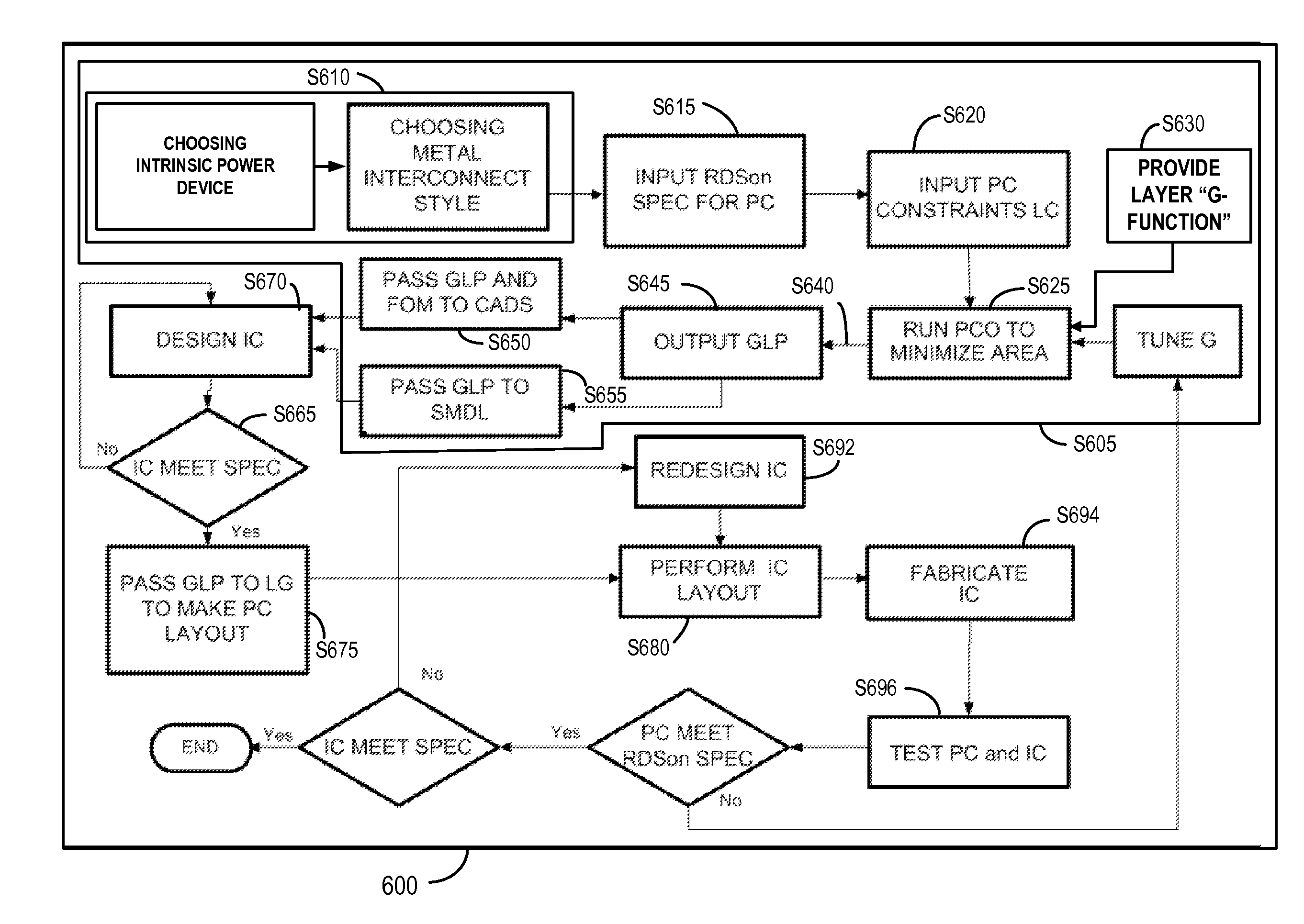
[0025]Embodiments of the present invention described herein provide a apparatus and method for optimized power cell synthesis. The apparatus and method employ compact analytical equations to accurately predict an optimization parameter value and to generate target parameter values which provide a power cell producing the optimization parameter value, when realized in silicon. Predictive optimization includes the effects of parasitic metal resistance and its variability with device layout. Analytical formulations can provide a closed-form solution that, when used judiciously, can find a global minimum in a continuous solution space. Compact analytical equations provide a representation of an ordered relationship among equation terms, which can describe a semiconductor device characteristic, and which can be exploited to optimize or to solve complex systems described by the analytical equations.

[0026]These models typically employ a small number circuit of elements, and are computation...


PUM


Abstract

Apparatus for providing semiconductor device with an analysis module to receive device information, a G-function processor producing an ordered relationship representation corresponding to an optimization parameter specification, and a power cell optimizer to produce an optimization parameter from the ordered relationship representation. A method for designing a semiconductor device includes receiving an optimization target specification; receiving an optimization parameter specification corresponding to an optimization parameter; receiving the target parameter; receiving a G-function corresponding to an ordered relationship representation; optimizing the optimization parameter specification as a function of the predetermined G-function; and producing at least one optimized geometric layout parameter (GLP) by the optimizing, wherein the at least one GLP corresponds to an optimized power cell.

Description

BACKGROUND[0001]1. Field of the Invention[0002]The present invention generally pertains to design of ICs containing large power transistors for low loss switching applications. In particular, power cells are designed to achieve low values of on-resistance (RDSon).[0003]2. Related Art[0004]Successful IC (integrated circuit) development for medium, high power, and very high power applications requires power transistors or cells that achieve very low values RDSon. IC applications including but not limited to power conversion, class-D audio amplifiers, power control for PC products, automotive, MEMS and display drivers leverage low RDSon to improve key figures of merit including energy efficiency, switching and conduction power loss, thermal problems, and switching frequency. The voltage levels of the transistors involved typically range from values of 5V to greater than 700V. The RDSon values required can reach into the sub 100 milli-ohm ranges.[0005]In general, the RDSon of a transist...

Claims


Application Information

Patent Timeline
Patent Type & Authority Patents(United States)
IPC IPC(8): G06F17/50
CPCG06F17/505G06F17/5068G06F2217/78G06F30/39G06F2119/06G06F30/00G06F30/327G06F30/398
Inventor CORDOVEZ, JUANVICTORY, JAMES
Owner GLOBALFOUNDRIES U S INC
Learn More