
Method and apparatus for automatically fixing double patterning loop violations

a technology of automatic fixing and loop, applied in the direction of photomechanical equipment, instruments, originals for photomechanical treatment, etc., can solve the problems of potential introduction of new design rule violations, etc., and achieve the effect of discounting the cost of shapes and reducing the cost of shapes

Active Publication Date: 2013-06-25
CADENCE DESIGN SYST INC
View PDF69 Cites 37 Cited by
  • Summary
  • Abstract
  • Description
  • Claims
  • Application Information

AI Technical Summary

Benefits of technology

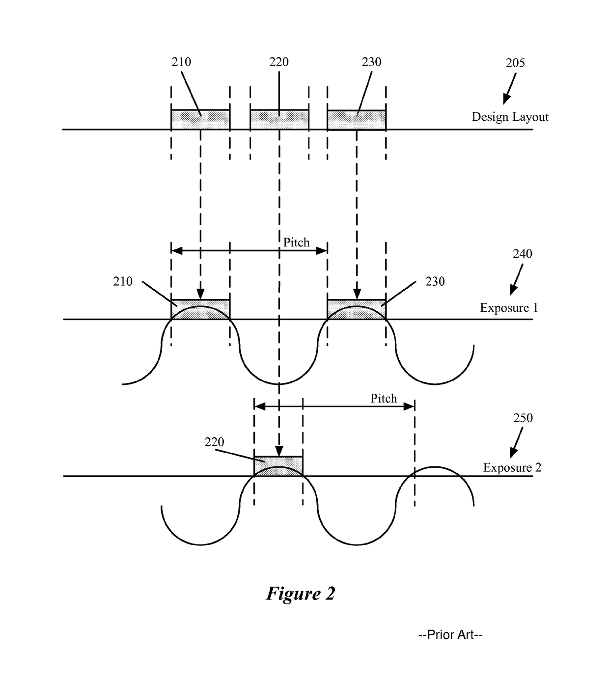
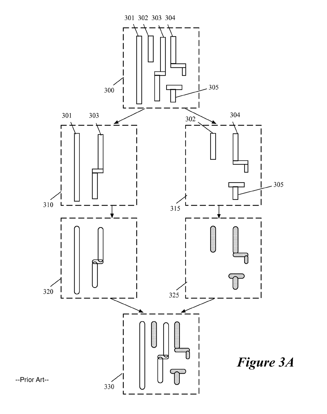
The patent describes a method for designing integrated circuits that reduces the cost of certain shapes in the circuit layout. The method calculates the cost of each shape based on its color and its distance from other shapes. If the shape is within a certain distance range and has a different color, the method assigns a lower cost to it. The method also suggests alternative colors for the shape if there is no color assigned to it. This helps to avoid design rules that would prevent the shape from being moved around in the circuit. Additionally, the method automatically decomposes the shape into multiple shapes to resolve double patterning loop issues. This decomposition is done by introducing splicing graphs on the shape and assigning colors to them based on their critical portions in the shape graph. The method minimizes the number of splicing graphs introduced and ensures that no two critical portions have the same color. Overall, this method improves the efficiency and accuracy of integrated circuit design.

Problems solved by technology

Some design solutions may introduce new design rule violations.
For each design solution generated for a DP loop violation, the method of some embodiments computes a cost of applying the solution to the IC design layout.
This accounts for the number of potential new design rule violations introduced by moving the shape.

Method used


Image

  • Method and apparatus for automatically fixing double patterning loop violations
  • Method and apparatus for automatically fixing double patterning loop violations
  • Method and apparatus for automatically fixing double patterning loop violations

Examples


Embodiment Construction

[0083]In the following detailed description of the invention, numerous details, examples, and embodiments of the invention are set forth and described. However, it will be clear and apparent to one skilled in the art that the invention is not limited to the embodiments set forth and that the invention may be practiced without some of the specific details and examples discussed.

I. OVERVIEW

A. Resolving a DP Loop Violation by Moving Shape Edge(s)

[0084]Some embodiments of the invention provide a method for automatically generating and prioritizing several design solutions that resolve a double patterning (DP) loop violation in an IC design layout. The method of some embodiments receives a DP loop violation marker and identifies pairs of edges of shapes that form a double patterning loop based on the DP loop violation marker. For each pair of edges that violates the design rule, the method generates one or more design solutions. Each design solution moves a single edge or both edges to r...


PUM

PropertyMeasurementUnit
sizesaaaaaaaaaa
threshold distanceaaaaaaaaaa
distanceaaaaaaaaaa

Abstract

A method for automatically generating and prioritizing several design solutions that resolve a double patterning (DP) loop violation in an IC design layout. The method of some embodiments receives a DP loop violation marker and identifies pairs of edges of shapes that form a double patterning loop based on the DP loop violation marker. For each pair of edges that violates the design rule, the method generates one or more design solutions. Each design solution moves a single edge or both edges to resolve the violation. The method of some embodiments computes the cost of applying each design solution to the IC design layout and prioritizes the generated solutions for all the identified pairs of edges based on the computed cost for each solution. The method in some embodiments then selects a solution from the prioritized solutions and applies the selected solution to the design layout.

Description

BACKGROUND[0001]An integrated circuit (“IC”) is a device (e.g., a semiconductor device) or electronic system that includes many electronic components, such as transistors, resistors, diodes, etc. These components are often interconnected to form multiple circuit components, such as gates, cells, memory units, arithmetic units, controllers, decoders, etc. An IC includes multiple layers of wiring that interconnect the IC's electronic and circuit components.[0002]Design engineers design ICs by transforming logical or circuit descriptions of the ICs' components into geometric descriptions, called design layouts. Design layouts typically include (1) circuit modules (i.e., geometric representations of electronic or circuit IC components) with pins and (2) interconnect lines (i.e., geometric representations of wiring) that connect the pins of the circuit modules. In this fashion, design layouts often describe the behavioral, architectural, functional, and structural attributes of the IC. T...

Claims


Application Information

Patent Timeline
Patent Type & Authority Patents(United States)
IPC IPC(8): G06F17/50G03F1/00G21K5/00
CPCG06F17/5081G03F7/70433G03F7/70466G03F1/00G21K5/00G06F30/398
Inventor SHARMA, KARUNCAO, MINRUEHL, ROLAND
Owner CADENCE DESIGN SYST INC
Learn More