Voltage compensation circuit
a voltage compensation circuit and circuit technology, applied in circuit-breaking switches, circuit-breaking switches for excess current, instruments, etc., can solve problems such as many electrical devices being damaged, and achieve the effect of greater winding thickness
- Summary
- Abstract
- Description
- Claims
- Application Information
AI Technical Summary
Benefits of technology
Problems solved by technology
Method used
Image
Examples
first embodiment
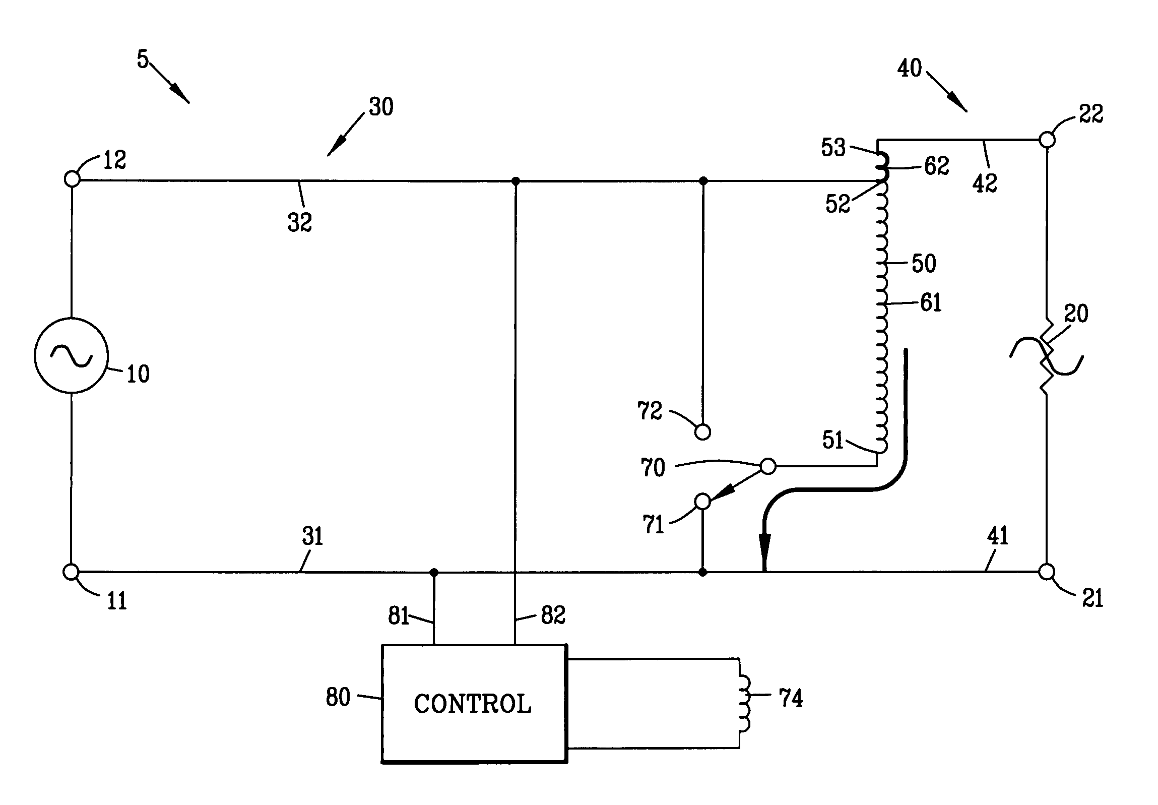
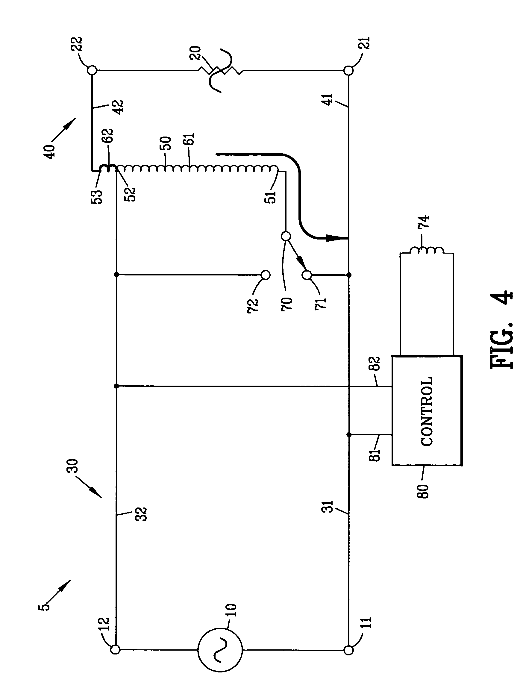
[0062]FIG. 4 is a circuit diagram of a voltage compensation circuit 5 of the present invention. The input AC voltage source 10 defines a first and a second input terminal 11 and 12. The input cable 30 comprises a first and a second input connector 31 and 32 whereas the output cable 40 comprises a first and a second output connector 41 and 42 for interconnecting the voltage compensation circuit 5 between the AC voltage source 10 and the load 20.
[0063]The voltage compensation circuit 5 comprises an autotransformer 50 having a first, second and a third transformer tap 51-53. The second transformer tap 52 of the autotransformer 50 is located between the first and third transformer taps 51 and 53. A first transformer winding 61 is defined between the first transformer tap 51 and the second transformer tap 52 of the autotransformer 50. A second transformer winding 62 is defined between the second transformer tap 52 and the third transformer tap 53 of the autotransformer 50.
[0064]In this e...
second embodiment
[0073]FIG. 6 is a circuit diagram of a voltage compensation circuit 105 of the present invention. Similar parts are labeled with similar reference characters raised by 100. In this example, the AC voltage source 110 is shown as a conventional 240-volt alternating current source. Although the AC voltage source 110 is shown as a conventional 240-volt AC voltage source, it should be understood that the AC voltage source 110 maybe any type of AC voltage source including one phase of a three phase electrical system.
[0074]The input AC voltage source 110 defines a first and a second input terminal 111 and 112 with a third input terminal 113 shown as a neutral terminal. The input cable 130 comprises first through third input connectors 131-133 whereas the output cable 140 comprises first through third output connector 141-143 for interconnecting the voltage compensation circuit 105 between the AC voltage source 110 and the load 120. In this example, the load 120 comprises a first and a seco...
third embodiment
[0092]Preferably, the voltage compensation circuit 205 is used for primarily regulating the voltage on the load 220C and secondarily for regulating the voltage on the loads 220A and 220B. The voltage compensation circuit 205 regulates the voltage on the loads 220A and 220B in accordance with the power requirement on the load 220C.
[0093]FIG. 10 is a circuit diagram of a fourth embodiment of a voltage compensation circuit 305 of the present invention. The fourth embodiment of the voltage compensation circuit 305 is a variation of the voltage compensation circuit 305 shown in FIGS. 8-9 with similar parts are labeled with similar reference characters raised by 100.
[0094]In this embodiment, the voltage compensation circuit 305 includes a single control 380. The control 380 sense an under voltage condition of the input AC voltage source between the first and the third terminals 311 and 313 and moves the switches 370A and 370B in unison into the first positions 371A and 371B. The under vol...
PUM
 Abstract
Description
Claims
Application Information
 - R&D
- Intellectual Property
- Life Sciences
- Materials
- Tech Scout
- Unparalleled Data Quality
- Higher Quality Content
- 60% Fewer Hallucinations
Browse by: Latest US Patents, China's latest patents, Technical Efficacy Thesaurus, Application Domain, Technology Topic, Popular Technical Reports.
© 2025 PatSnap. All rights reserved.Legal|Privacy policy|Modern Slavery Act Transparency Statement|Sitemap|About US| Contact US: help@patsnap.com


