Directional coupler
a technology of directional couplers and coupling lines, applied in the direction of coupling devices, electrical devices, waveguides, etc., can solve the problems of manufacturing variations, significant increase in reflection loss in chips, degradation of reflection loss characteristics of coupled lines, etc., and achieve good reflection loss characteristics
- Summary
- Abstract
- Description
- Claims
- Application Information
AI Technical Summary
Benefits of technology
Problems solved by technology
Method used
Image
Examples
first embodiment
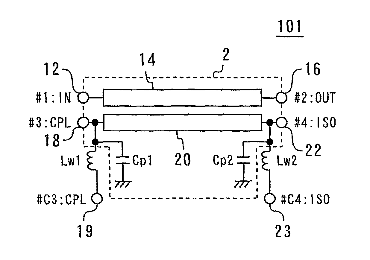
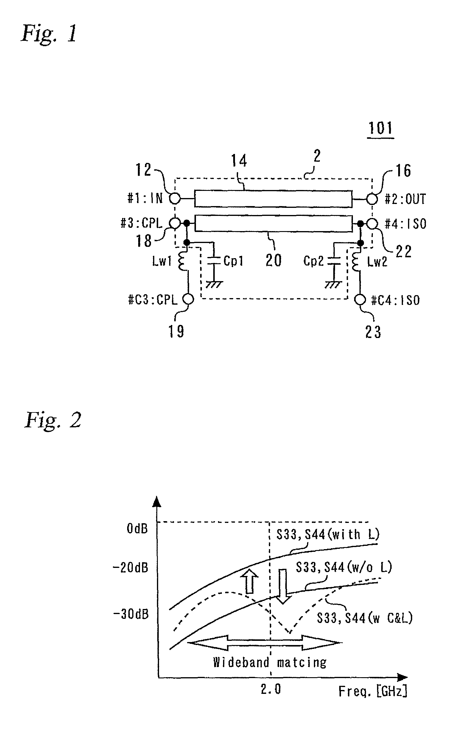
[0039]Preferred embodiments of the present invention will be described in connection with a configuration in which a chip with a directional coupler thereon is mounted on a module substrate or a printed board. The chip with a directional coupler thereon can be manufactured by a GaAs-HBT process, a GaAs-BiFET (HBT+FET or HBT+HEMT) process, or a GaAs-HEMT / FET process. The coupled port and the isolated port of the directional coupler are both connected to a component or device outside the module. This connection is accomplished through inductive connecting elements, such as bonding wires, and transmission lines in the module substrate. It should be noted that the embodiments described below can also be applied to directional couplers manufactured by a Si-based process. Further, these embodiments are suitable as applied to the case where the coupled lines (also referred to as the “sub-lines”) of the directional couplers in a multiband-capable terminal are connected in series with one an...
second embodiment
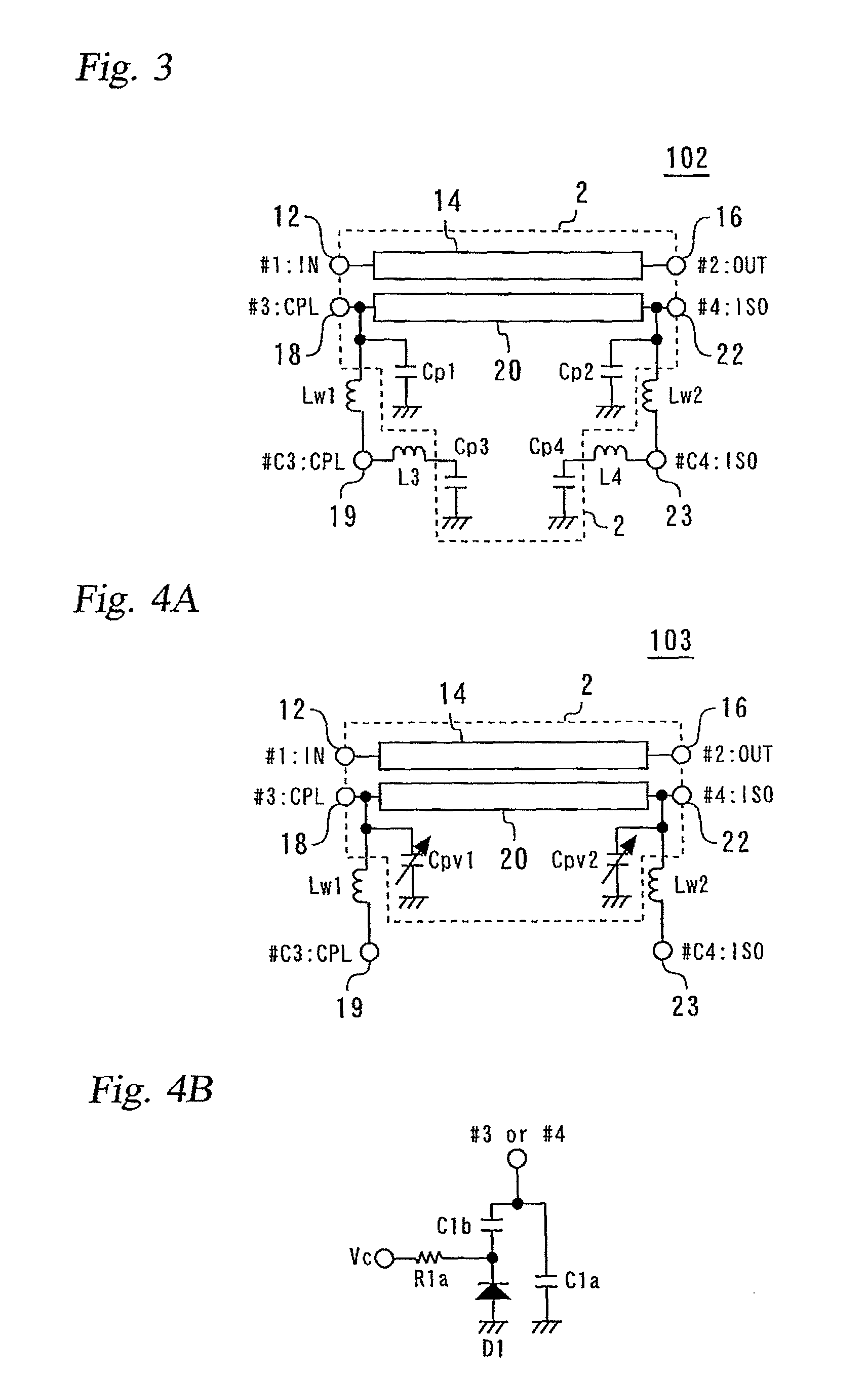
[0047]FIG. 3 is a circuit diagram of a directional coupler 102 according to a second embodiment of the present invention. This directional coupler 102 differs from the directional coupler 101 of the first embodiment in that it additionally includes inductances L3 and L4 and capacitive elements Cp3 and Cp4. L3 and L4 are the parasitic inductances of connecting elements. That is, each matching circuit to the coupled line 20 of the directional coupler 102 is an LCLC circuit and includes 4 components, whereas each matching circuit to the coupled line of the directional coupler 101 of the first embodiment shown in FIG. 1 is an LC circuit and includes 2 components. This increase in the number of components allows the reflection loss characteristics of the coupled line to be improved over a wider band, as compared with the first embodiment.
third embodiment
[0048]FIG. 4, which includes FIGS. 4A and 4B, is a circuit diagram of a directional coupler 103 according to a third embodiment of the present invention. This directional coupler 103 differs from the directional coupler 101 shown in FIG. 1 in that the capacitive elements Cp1 and Cp1 are replaced by variable capacitance elements Cpv1 and Cpv2, respectively, as shown in FIG. 4A. FIG. 4B shows the actual circuit configuration of the variable capacitance elements Cpv1 and Cpv2. As shown in FIG. 4B, each of Cpv1 and Cpv2 includes a resistance R1a, a capacitance Cb1, a variable capacitance diode D1, and a fixed value capacitance C1a. The capacitance of Cpv1 and Cpv2 can be varied by varying the control voltage Vc. This makes it possible to vary the reflection characteristics of the coupled line (which characteristics correspond to those indicated by the reference symbol “S33, S44 (w-C&L)” in FIG. 2), allowing the characteristics to be adjusted finely or over a selected band even after mou...
PUM
 Abstract
Description
Claims
Application Information
 - R&D
- Intellectual Property
- Life Sciences
- Materials
- Tech Scout
- Unparalleled Data Quality
- Higher Quality Content
- 60% Fewer Hallucinations
Browse by: Latest US Patents, China's latest patents, Technical Efficacy Thesaurus, Application Domain, Technology Topic, Popular Technical Reports.
© 2025 PatSnap. All rights reserved.Legal|Privacy policy|Modern Slavery Act Transparency Statement|Sitemap|About US| Contact US: help@patsnap.com


