Compound semiconductor epitaxial substrate and method for producing the same

a technology of semiconductor epitaxial substrate and semiconductor, applied in the direction of basic electric elements, electrical apparatus, semiconductor devices, etc., can solve the problems of power loss, limit the reduction of transient resistance of electronic devices, etc., and achieve the effect of improving electron mobility characteristics

Inactive Publication Date: 2011-05-03
SUMITOMO CHEM CO LTD
View PDF15 Cites 94 Cited by
  • Summary
  • Abstract
  • Description
  • Claims
  • Application Information

AI Technical Summary

Benefits of technology

[0015]An object of the present invention is to provide a higher-performance compound semiconductor epitaxial substrate having improved electron mobility characteristics and a method for producing the same.

Problems solved by technology

Accordingly, there have been limitations on achieving reductions in transient resistance and power loss of the electronic device, and increasing the levels of characteristics of the electronic device to levels higher than the present levels by increasing the electron mobility.
However, from the viewpoint that the characteristics of the electronic device are improved as the two-dimensional electron gas concentration and the electron mobility have higher values in the compound semiconductor epitaxial substrate having the channel layer in which electrons travel such as the epitaxial substrate having the p-HEMT structure, the respective values of the two-dimensional electron gas concentration and the electron mobility are not satisfactory in the field to which devices for high frequency or the like are applied to, and therefore an epitaxial substrate having improved electron mobility characteristics with high two-dimensional electron gas concentration and high electron mobility has been in demand.

Method used


Image

  • Compound semiconductor epitaxial substrate and method for producing the same
  • Compound semiconductor epitaxial substrate and method for producing the same
  • Compound semiconductor epitaxial substrate and method for producing the same

Examples


example

[0060]The present invention will be described by using an example. However, the present invention is not limited to the present example.

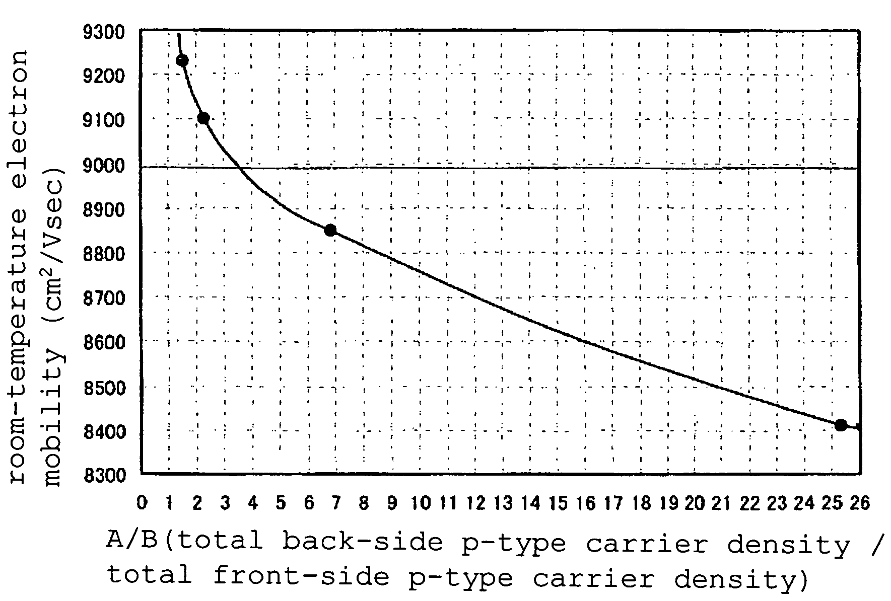
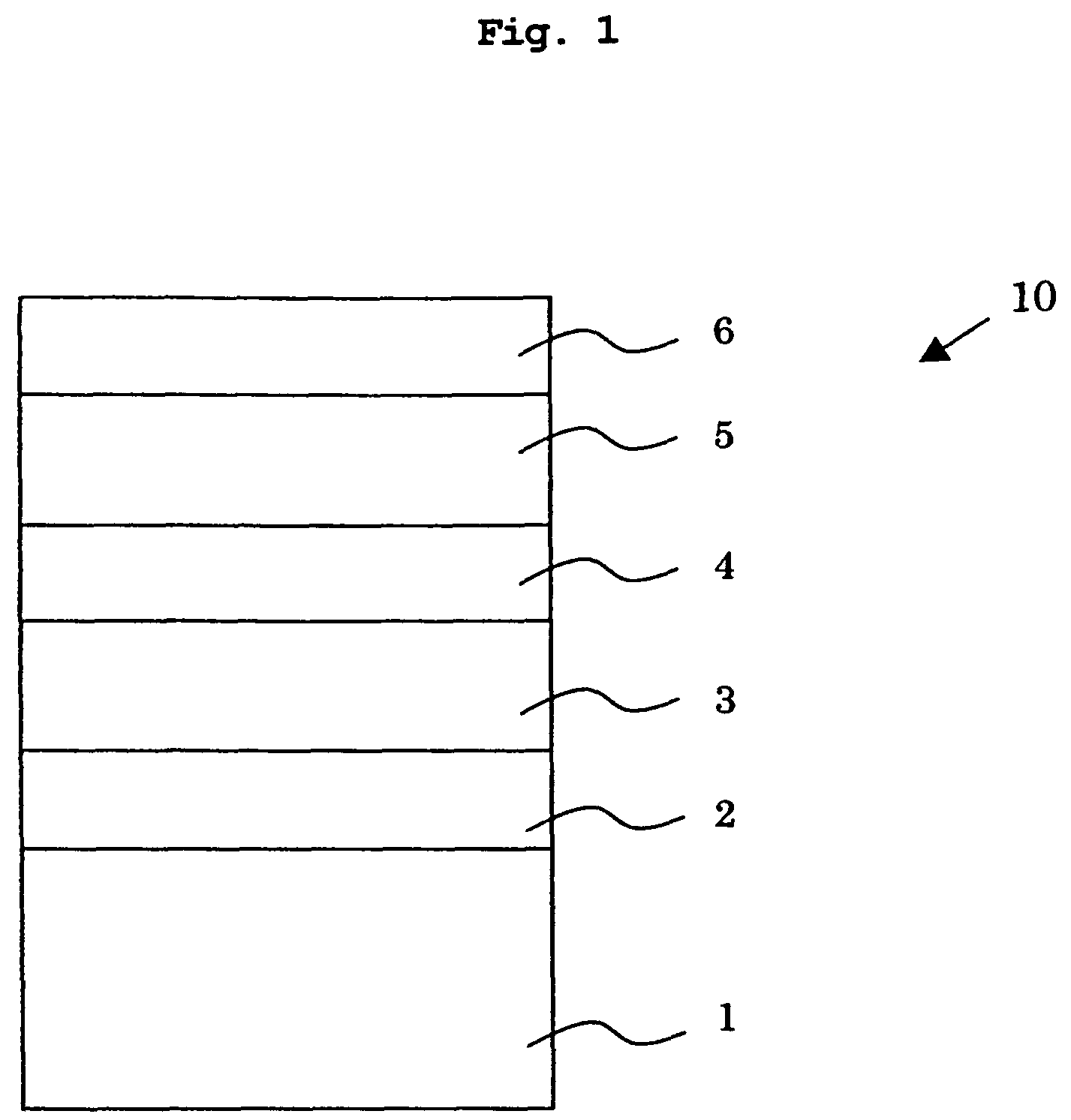
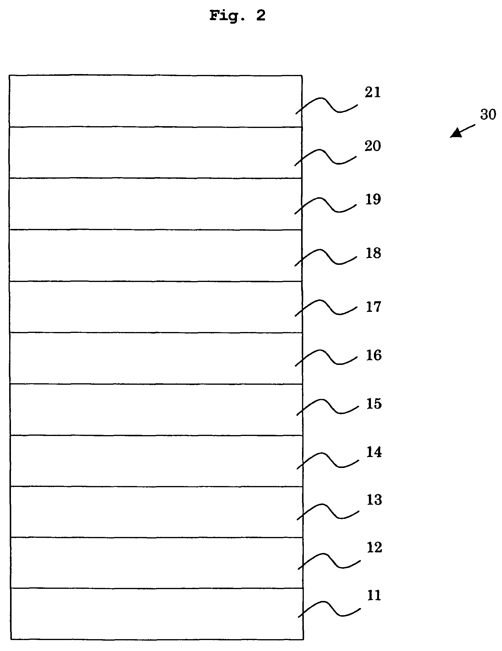
[0061]A compound semiconductor epitaxial substrate 30 for a p-HEMT illustrated in FIG. 2 was produced by growing individual layers on the semi-insulating GaAs template. The compound semiconductor epitaxial substrate 30 illustrated in FIG. 2 comprises

a semi-insulating GaAs template 11,

a buffer layer 12 (p-Al0.25Ga0.75As, thickness: 100 nm, carrier density: 1 to 200E15 / cm3),

a buffer layer 13 (p-Al0.20Ga0.80As, thickness: 50 nm, carrier density: 2E16 / cm3),

a back-side electron supply layer 14 (n-Al0.20Ga0.80As, thickness: 4 nm, carrier density: 3E18 / cm3),

a back-side spacer layer 15 (p-Al0.20Ga0.80As, thickness: 3 nm, carrier density: 2E16 / cm3),

a back-side spacer layer 16 (i-GaAs, thickness: 6 nm),

a channel layer 17 (i-In0.35Ga0.65As, thickness: 6 nm),

a front-side spacer layer 18 (i-GaAs, thickness: 6 nm),

a front-side spacer layer 19 (p-Al0.20Ga0.80As, t...


PUM


Abstract

There are provided a higher-performance compound semiconductor epitaxial substrate having improved electron mobility characteristics and its production method. The compound semiconductor epitaxial substrate includes a channel layer in which electrons travel and an epitaxial layer on each of a front side and a back side of the channel layer, wherein a total p-type carrier concentration A ( / cm2) per unit area in the epitaxial layer on the back side of the channel layer and a total p-type carrier concentration B ( / cm2) per unit area in the epitaxial layer on the front side of the channel layer satisfy the following expression (1):0<A / B≦3.5  (1)wherein A=(a concentration of all p-type carriers in an active state due to an acceptor impurity contained in the epitaxial layer on the back side of the channel layer)×(a total thickness of the epitaxial layer on the back side), and B=(a concentration of all p-type carriers in an active state due to an acceptor impurity contained in the epitaxial layer on the front side of the channel layer)×(a total thickness of the epitaxial layer on the front side).

Description

CROSS-REFERENCE TO RELATED APPLICATIONS[0001]This is a U.S. National Phase of International Application PCT / JP2007 / 061236, filed May 28, 2007, and claims the benefit of priority under 35 U.S.C. §119 based on Japanese Application No. 2006-150768, filed May 31, 2006, the entire disclosures of which applications are hereby incorporated herein by reference.TECHNICAL FIELD[0002]The present invention relates to a compound semiconductor epitaxial substrate which is preferable for use in the production of various electronic devices such as a field effect transistor (hereinafter referred to as FET), a high electron mobility transistor (hereinafter referred to as HEMT), and the like, and a method for producing the same.BACKGROUND ART[0003]In recent years, with an advantage of being capable of a super-high-speed and high-frequency operation, various electronic devices using a group III-V compound semiconductor mainly represented by GaAs have been dramatically developed by being used in high-fr...

Claims


Application Information

Patent Timeline
Patent Type & Authority Patents(United States)
IPC IPC(8): H01L29/66
CPCH01L29/66462H01L21/02395H01L21/02463H01L21/0262H01L21/02546H01L21/2056H01L21/18H01L29/201H01L29/778H01L29/812
Inventor NAKANO, TSUYOSHI
Owner SUMITOMO CHEM CO LTD
Why Eureka
Try Eureka