
Display device

a display device and display screen technology, applied in the field of display devices, can solve problems such as contrast deterioration and contrast deterioration, and achieve the effects of preventing contrast deterioration, preventing contrast deterioration, and simplifying configuration

Inactive Publication Date: 2010-09-21
JOLED INC
View PDF8 Cites 5 Cited by
  • Summary
  • Abstract
  • Description
  • Claims
  • Application Information

AI Technical Summary

Benefits of technology

[0016]There is a need for the present invention to provide a display device that is allowed to prevent contrast deterioration due to floating black and sinking black with a simple configuration.
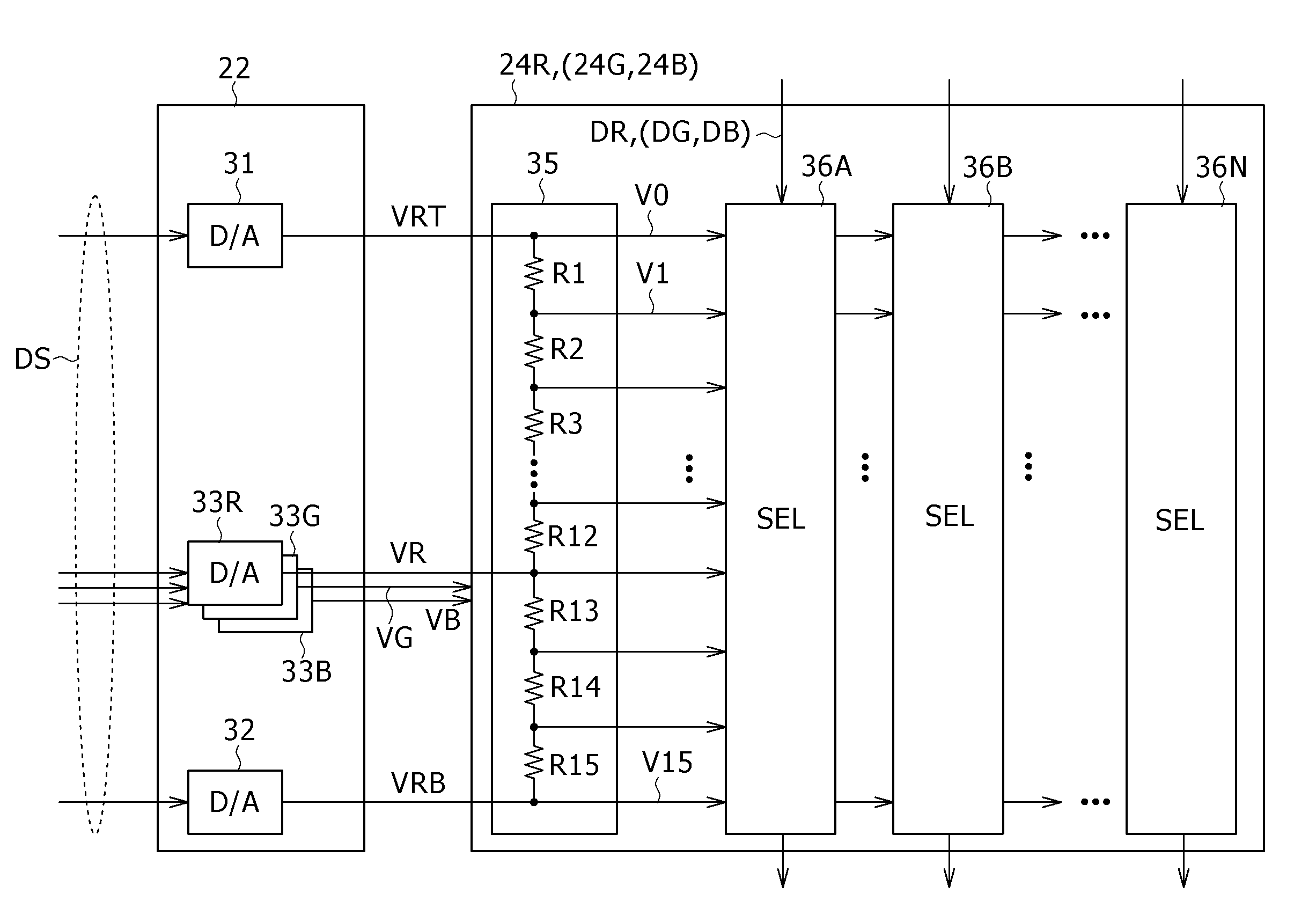
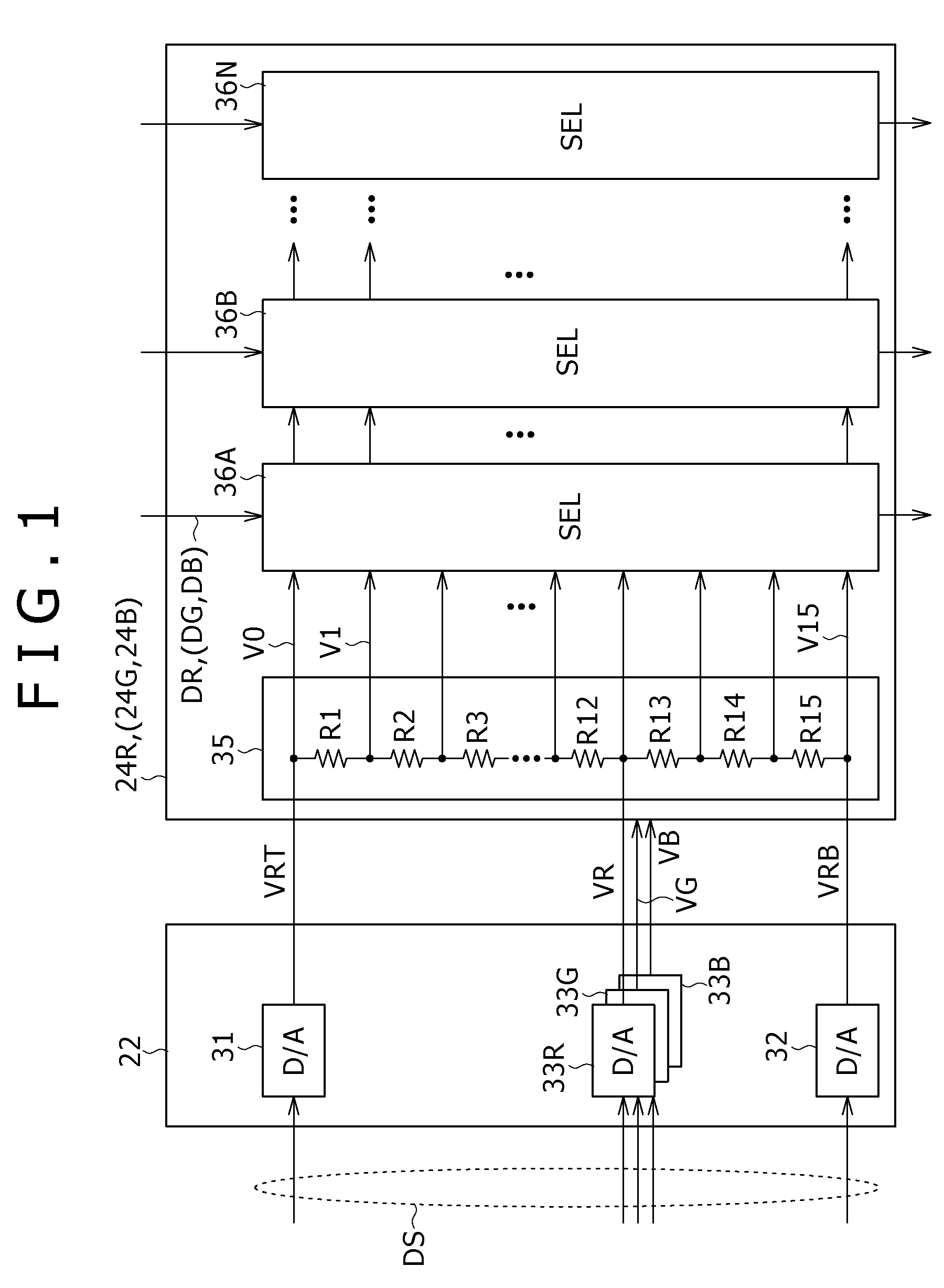
[0018]In this configuration, at least the basic reference voltage corresponding to the black level is supplied to the plurality of voltage divider circuits in common, and thus a simplified configuration can be achieved. In addition, the basic reference voltages closer to the black level than the voltage corresponding to the center value of the drive signal are each supplied to a respective one of the plurality of voltage divider circuits for a respective one of the color data. This can prevent floating black and sinking black in the pixels of the respective colors and thus can prevent contrast deterioration.
[0019]According to the embodiment of the present invention, contrast deterioration due to floating black and sinking black can be prevented with a simple configuration.

Problems solved by technology

However, in a practical organic EL element 2, the luminance value on the black side often deviates to a higher value from its ideal characteristic expressed by Equation (2), which leads to contrast deterioration.
However, in practice, it often changes depending on the current, and very often changes in a lower-current region in particular.
When the efficiency decreases on the lower current side, the black side sinks (becomes darker), contrary to the floating black, and thus the contrast deteriorates.

Method used


Image

  • Display device
  • Display device
  • Display device

Examples


first embodiment

(1) Configuration of Embodiment

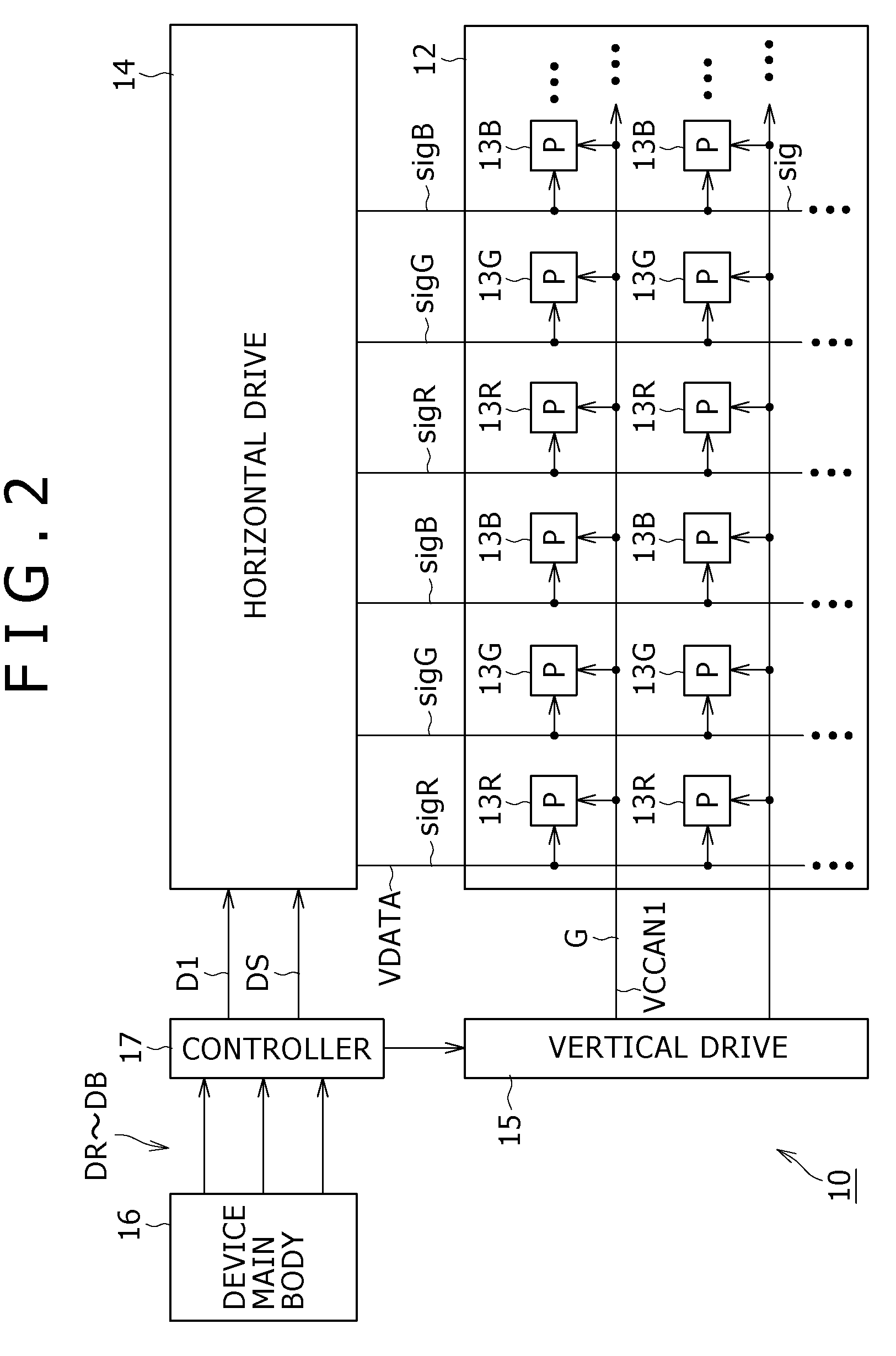
[0038]FIG. 2 is a block diagram showing a display device according to a first embodiment of the present invention. In this display device 10, TFTs and so on are sequentially fabricated on an insulating substrate such as a glass substrate, so that red, green, and blue pixels 13R, 13G, and 13B are arranged in a matrix for formation of a display part 12. In the display device 10, each of the pixels 13R, 13G, and 13B in this display part 12 is connected to a horizontal drive circuit 14 and a vertical drive circuit 15 via a signal line (column line) sig (sigR, sigG, sigB) and a scan line (row line) G, respectively. In this display device 10, the pixels 13R, 13G, and 13B are sequentially selected by the vertical drive circuit 15, and the grayscales of the respective pixels 13R, 13G, and 13B are set based on drive signals from the horizontal drive circuit 14, so that a desired color image is displayed.

[0039]For this displaying, in the display device 10, image...

second embodiment

[0058]FIG. 5 is a connection diagram showing a pixel applied to a display device according to a second embodiment of the present invention. In a pixel 32 of this embodiment, a drive transistor Tr2 is formed of an n-channel MOS transistor. Therefore, the respective components are so formed that, as shown in FIG. 6 as comparison with FIG. 4, the relationship between the light emission luminance of the pixel and the potential of a signal line sig will be opposite to that in the display device 10 of the above-described first embodiment.

[0059]Also in the case in which a drive transistor is formed of an n-channel MOS transistor like in this embodiment, the same advantages as those by the first embodiment can be achieved.

third embodiment

[0060]FIGS. 7 and 8 are block diagrams showing, based on comparison with FIGS. 1 and 3, a partial configuration of a display device according to a third embodiment of the present invention. In this display device, for the respective color data, a basic reference voltage generation circuit 42 generates basic reference voltages VRTR, VRTG, and VRTB for setting of the white levels for red, green, and blue, respectively. Furthermore, red, green, and blue digital-analog converters 44R, 44G, and 44B produce reference voltages V0 to V15 by using these basic reference voltages VRTR, VRTG, and VRTB for setting of the white levels for red, green, and blue. This can adjust the white level as well as an intermediate level near the black level on a color-by-color basis.

[0061]According to this embodiment, not only an intermediate level near the black level but also the white level can be adjusted on a color-by-color basis, which can further enhance the color reproducibility.


PUM


Abstract

In an embodiment of the present invention, basic reference voltages VRT, VRB, VR, VG, and VB are divided by resistors to produce plural reference voltages V0 to V15, and voltages are selected from these plural reference voltages V0 to V15 for digital-analog conversion processing of image data DR, DG, and DB. At least the basic reference voltage VRB for the black level is shared by the respective color data DR, DG, and DB. The basic reference voltages VR, VG, and VB for setting of an intermediate grayscale closer to the black level can be varied individually for each of the color data DR, DG, and DB. When this embodiment is applied to a display device employing current-driven light-emitting elements such as organic EL elements, contrast deterioration due to floating black and sinking black can be prevented with a simple configuration.

Description

CROSS REFERENCES TO RELATED APPLICATIONS[0001]The present invention contains subject matter related to Japanese Patent Application JP 2006-283412 filed with the Japan Patent Office on Oct. 18, 2006, the entire contents of which being incorporated herein by reference.BACKGROUND OF THE INVENTION[0002]1. Field of the Invention[0003]The present invention relates to display devices and can be applied to a display device that employs current-driven light-emitting elements such as organic electro luminescence (EL) elements. In an embodiment of the present invention, basic reference voltages are divided by resistors to thereby produce plural reference voltages, and voltages are selected from the plural reference voltages for digital-analog conversion processing of image data. In particular, at least the basic reference voltage for the black level is shared by the respective color data, and the basic reference voltages for setting of an intermediate grayscale closer to the black level can be...

Claims


Application Information

Patent Timeline
Patent Type & Authority Patents(United States)
IPC IPC(8): G09G3/30
CPCG09G3/3208G09G3/3291G09G2310/027G09G2320/0271G09G2320/043G09G2330/028G09G3/30H04N9/69G09G3/32G09G3/20
Inventor ASANO, MITSURU
Owner JOLED INC
Learn More