Electrophoretic display device and driving method thereof
a display device and display device technology, applied in the direction of instruments, static indicating devices, etc., can solve the problems of image contrast tending to be deteriorated, achieve the effect of preventing luminance level shift and contrast deterioration, preventing and improving image persistence and contrast, and improving contras
- Summary
- Abstract
- Description
- Claims
- Application Information
AI Technical Summary
Benefits of technology
Problems solved by technology
Method used
Image


Examples
specific examples
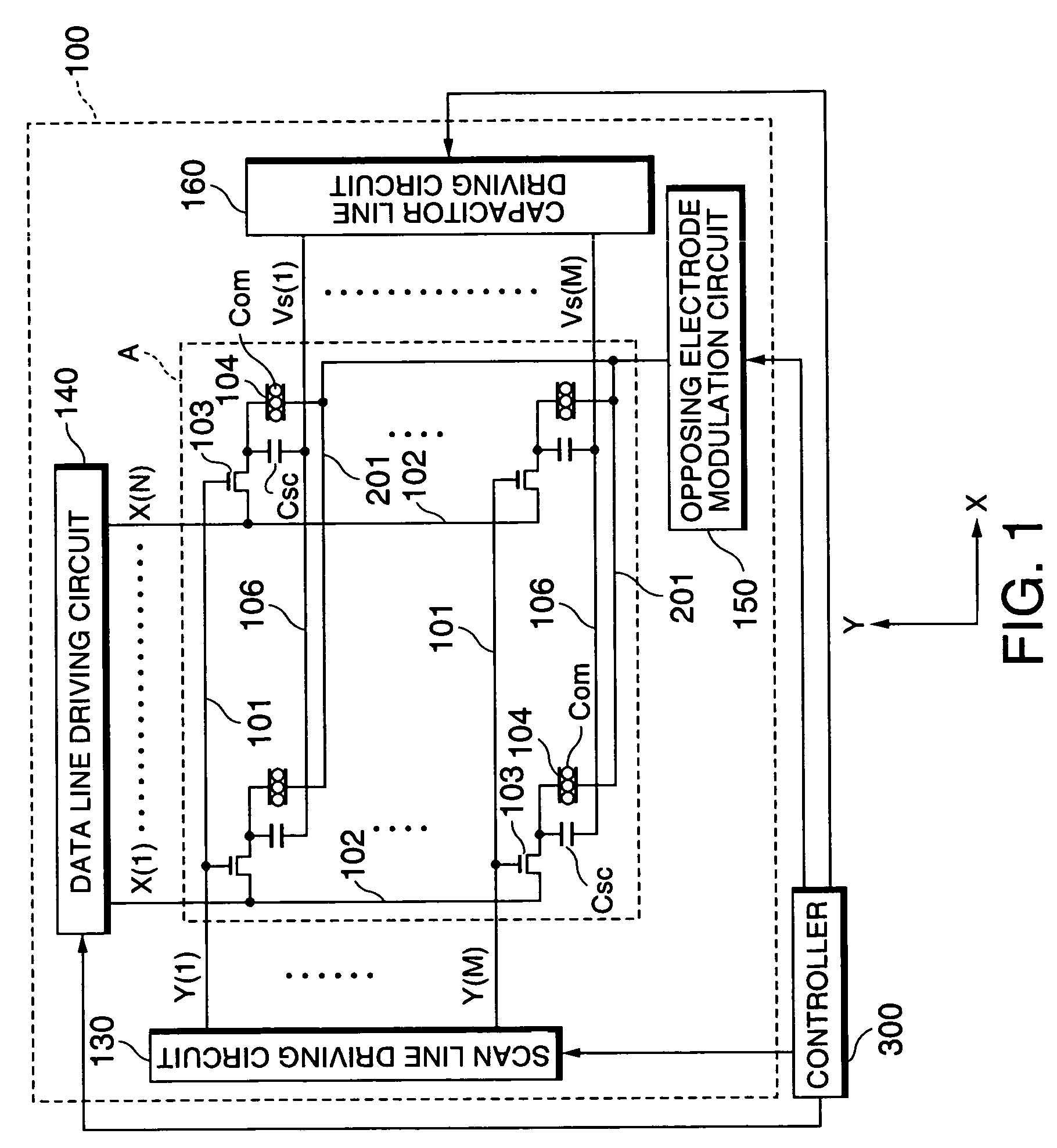
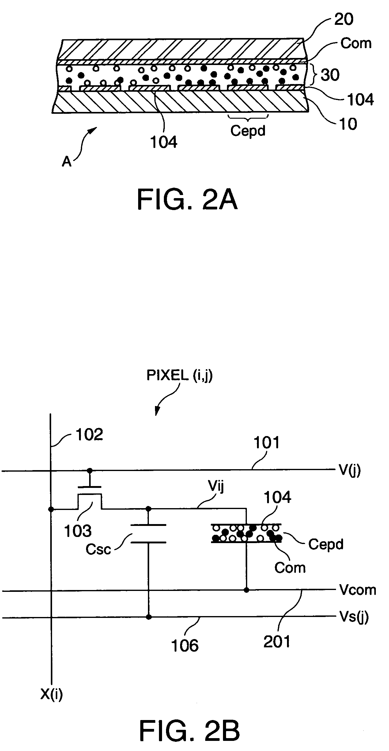
[0162]FIGS. 6 through 9 schematically show the states of the electric field between the common electrode and the pixel electrode and the states of the electrophoretic particle in the above described embodiment according to various display conditions. In FIGS. 6 through 9, FIG. A shows a state of a previous screen, FIG. B shows a state of the negatively charged white particle reset, FIG. C shows the standby state, FIG. D shows the writing state and FIG. E shows the data hold state. In the figures, the upper electrode is the common electrode Com and the lower electrode is the pixel electrode. Voltage of each electrode and the voltage values used in the above described embodiments are also shown in the figures. The voltage of the pixel electrode in the pixel (i, j) is denoted as Vij.
[0163]FIG. 6 shows the case where the negatively charged particle reset is performed when the pixel of the previous screen is black and the white writing is then carried out. If the negatively charged parti...
PUM
 Abstract
Description
Claims
Application Information
 - R&D
- Intellectual Property
- Life Sciences
- Materials
- Tech Scout
- Unparalleled Data Quality
- Higher Quality Content
- 60% Fewer Hallucinations
Browse by: Latest US Patents, China's latest patents, Technical Efficacy Thesaurus, Application Domain, Technology Topic, Popular Technical Reports.
© 2025 PatSnap. All rights reserved.Legal|Privacy policy|Modern Slavery Act Transparency Statement|Sitemap|About US| Contact US: help@patsnap.com