Delay locked loop for an FPGA architecture
a technology of delay lock and fpga, applied in the direction of generating/distributing signals, instruments, computing, etc., can solve the problems of clock signal unacceptably degrade, limited fanout of a single source, and other problems such as clock degradation, to achieve the effect of reducing the number of clock trees
- Summary
- Abstract
- Description
- Claims
- Application Information
AI Technical Summary
Problems solved by technology
Method used
Image
Examples
Embodiment Construction
[0022]Those of ordinary skill in the art will realize that the following description of the present invention is illustrative only and not in any way limiting. Other embodiments of the invention will readily suggest themselves to such skilled persons.
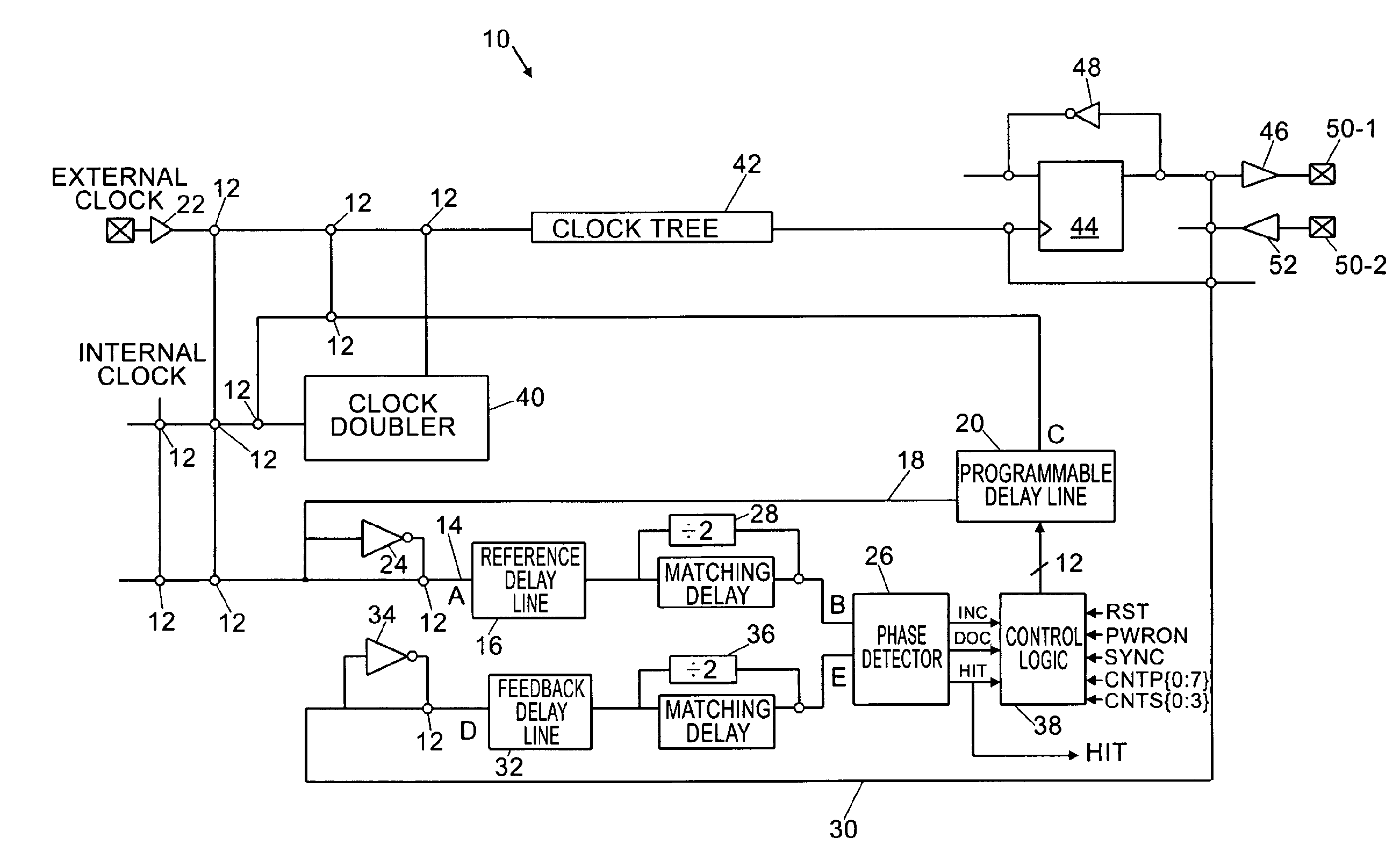
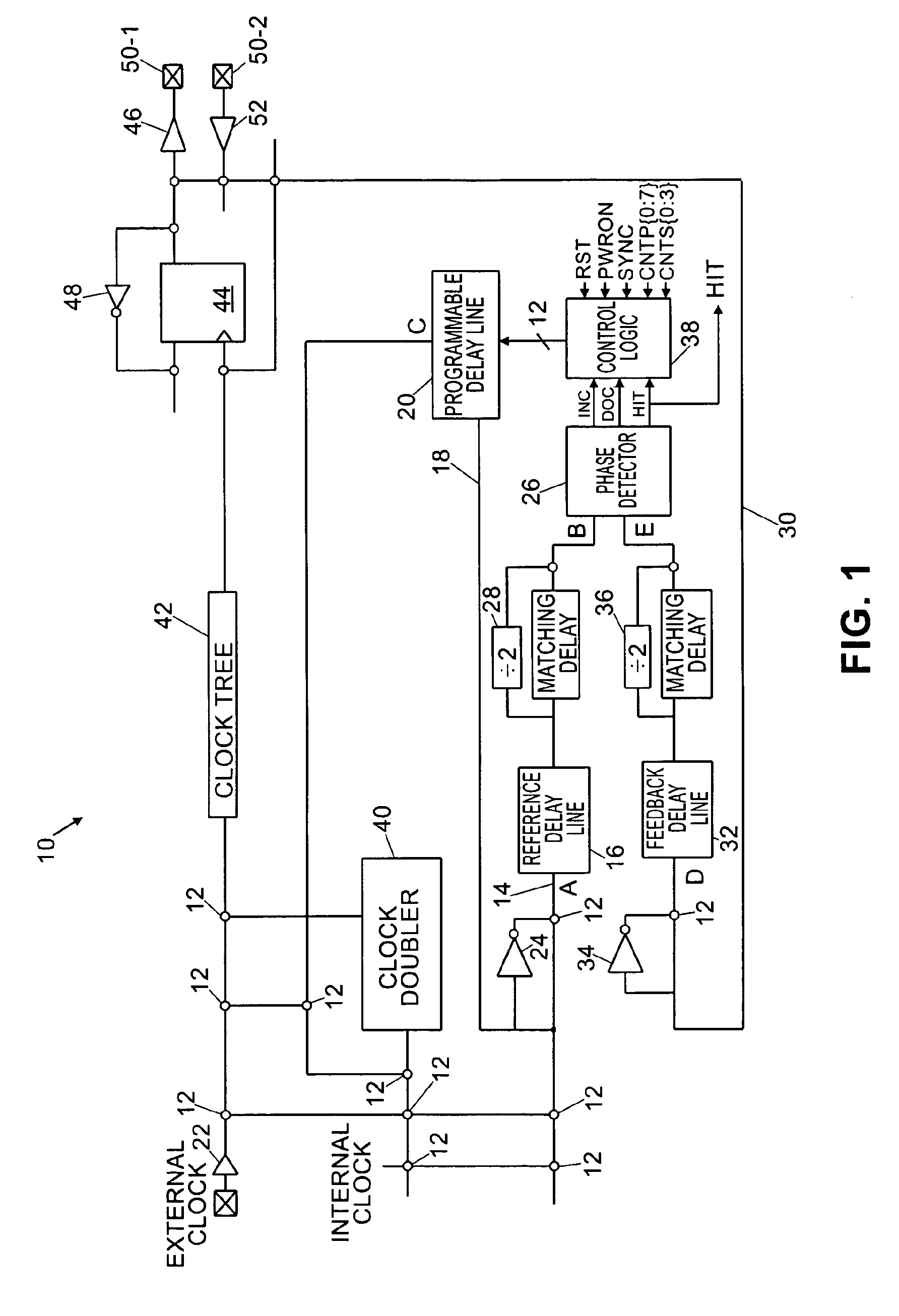
[0023]In FIG. 1, a diagram of a DLL 10 and some additional circuit elements according to the present invention are illustrated. Various portions of the diagram in FIG. 1 may be connected by programmable interconnect elements 12 that are illustrated as open circles. It will be appreciated by those of ordinary skill in the art that programmable interconnect elements 12 suitable for use according to the present invention may be any of several one time programmable or reprogrammable elements, including antifuses, EEPROM bits, SRAM bits or transistors.
[0024]In FIG. 1, a reference clock signal is supplied by either an INTERNAL CLOCK signal or EXTERNAL CLOCK signal that is programmably coupled by a programmable interconnect element 12 to the i...
PUM
 Abstract
Description
Claims
Application Information
 - R&D
- Intellectual Property
- Life Sciences
- Materials
- Tech Scout
- Unparalleled Data Quality
- Higher Quality Content
- 60% Fewer Hallucinations
Browse by: Latest US Patents, China's latest patents, Technical Efficacy Thesaurus, Application Domain, Technology Topic, Popular Technical Reports.
© 2025 PatSnap. All rights reserved.Legal|Privacy policy|Modern Slavery Act Transparency Statement|Sitemap|About US| Contact US: help@patsnap.com


