IMF cover for a portable electronic device
a technology for electronic devices and front covers, applied in the field of front covers for portable electronic devices, can solve the problems of water entering the holes, affecting the function of the key, damage to the phone, etc., and achieve the effect of simplifying the mounting process of the portable electronic devi
- Summary
- Abstract
- Description
- Claims
- Application Information
AI Technical Summary
Benefits of technology
Problems solved by technology
Method used
Image
Examples
first embodiment
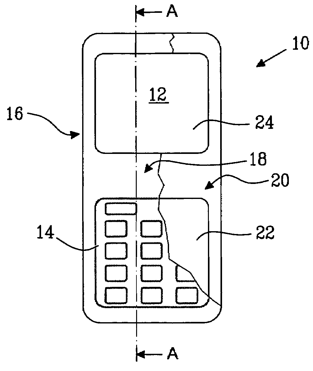
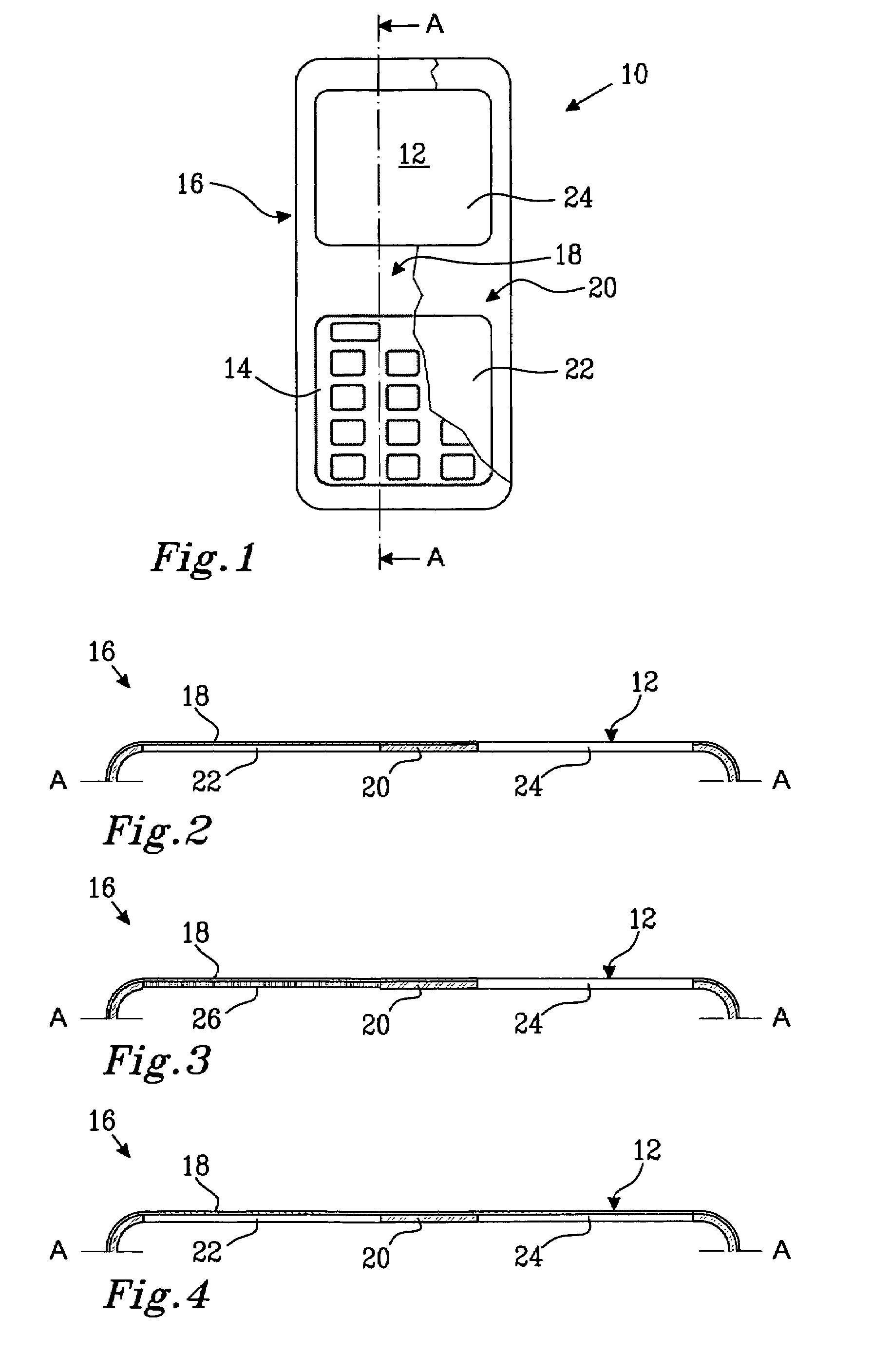
[0042]FIG. 2 shows a cross-sectional view of the front cover 16 according to the present invention. The front cover 16 has a thin top layer 18 of 0.175 mm thick flexible plastic film which is bonded to a bottom layer 20 of 1.2 mm thick stiff plastic material. This structure is a so-called IMF structure (In Mould Foil) structure, which means that the two layers are moulded together. The bottom layer 20 is here intended to face inwards towards the interior of the phone, while the top layer 18 is intended to face outwards towards a user of the phone. The bottom layer 22 is furthermore provided with a first opening 22 and a second opening 24. The second opening 24 is provided for allowing a user to view a display (not shown) for this reason there is furthermore a window 12 of transparent plastic material provided above the second opening 24 and covering the display in order to protect it. The first opening 22 is provided in order to allow the provision of a keypad providing one or more ...
second embodiment
[0047]the present invention is directed towards solving this / these problems.
[0048]FIG. 3 shows a cross-sectional view of the front cover 16 according to the second embodiment of the present invention. In many respects this embodiment is identical to the first embodiment. The only difference is that in the first opening, below the top layer 18, there is provided a patch layer 26 of 0.4 mm thick flexible thermo elastic or silicon material. This patch layer 26 covers the whole first opening and is furthermore bonded to both the top layer 18 and the bottom layer 20. It may however be sufficient that it is only bonded to the top layer 18. The patch layer 26 has been produced in the same moulding process and thus it is moulded to both the top layer 18 and the bottom layer 20.
[0049]The provision of this patch layer 26 has shown to provide even surfaces, which thus provides a much more aesthetically pleasing cover. Because of this the key input process is also improved.
[0050]The patch layer...
PUM
| Property | Measurement | Unit |
|---|---|---|
| thickness | aaaaa | aaaaa |
| thickness | aaaaa | aaaaa |
| thickness | aaaaa | aaaaa |
Abstract
Description
Claims
Application Information
 - R&D
- Intellectual Property
- Life Sciences
- Materials
- Tech Scout
- Unparalleled Data Quality
- Higher Quality Content
- 60% Fewer Hallucinations
Browse by: Latest US Patents, China's latest patents, Technical Efficacy Thesaurus, Application Domain, Technology Topic, Popular Technical Reports.
© 2025 PatSnap. All rights reserved.Legal|Privacy policy|Modern Slavery Act Transparency Statement|Sitemap|About US| Contact US: help@patsnap.com


