
Impedance measuring apparatus of package substrate and method for the same

a technology of impedance measurement and substrate, which is applied in the direction of resistance/reactance/impedence, measurement devices, instruments, etc., can solve the problems of loss and measurement error, phase difference, and large measurement error in a lower frequency range, and achieve the effect of sufficient accuracy

Inactive Publication Date: 2007-11-06
RENESAS ELECTRONICS CORP
View PDF5 Cites 5 Cited by
  • Summary
  • Abstract
  • Description
  • Claims
  • Application Information

AI Technical Summary

Benefits of technology

The patent text describes an impedance measuring apparatus for measuring RF signals on a package substrate. The apparatus includes multiple RF probes and a processing unit. The apparatus can accurately measure the RF impedance and phase difference of the signal within a limited frequency range. It can also calibrate the phase difference based on the thickness of the package substrate. The apparatus can be used in the GHz frequency range and can measure the RF impedance of a power source / GND line. The apparatus can be calibrated using a calibration substrate and a fine driving mechanism. The apparatus can be controlled using a mechanical controller. The technical effect of the invention is to provide an accurate and reliable method for measuring RF impedance on a package substrate.

Problems solved by technology

Therefore, the electric distance causes a phase difference, a loss and a measurement error.
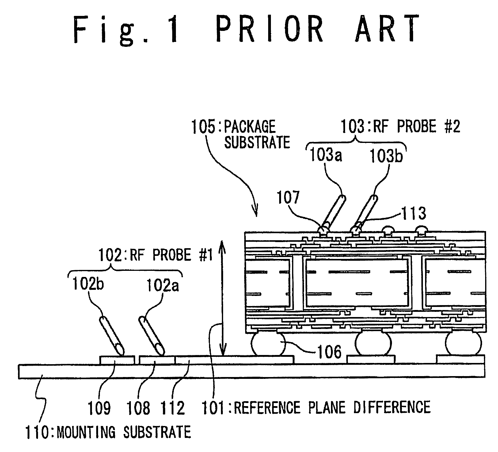
Further, when the object to be measured in FIG. 1 is a power source / GND line, there will be a larger measurement error in a lower frequency range.

Method used


Image

  • Impedance measuring apparatus of package substrate and method for the same
  • Impedance measuring apparatus of package substrate and method for the same
  • Impedance measuring apparatus of package substrate and method for the same

Examples


first embodiment

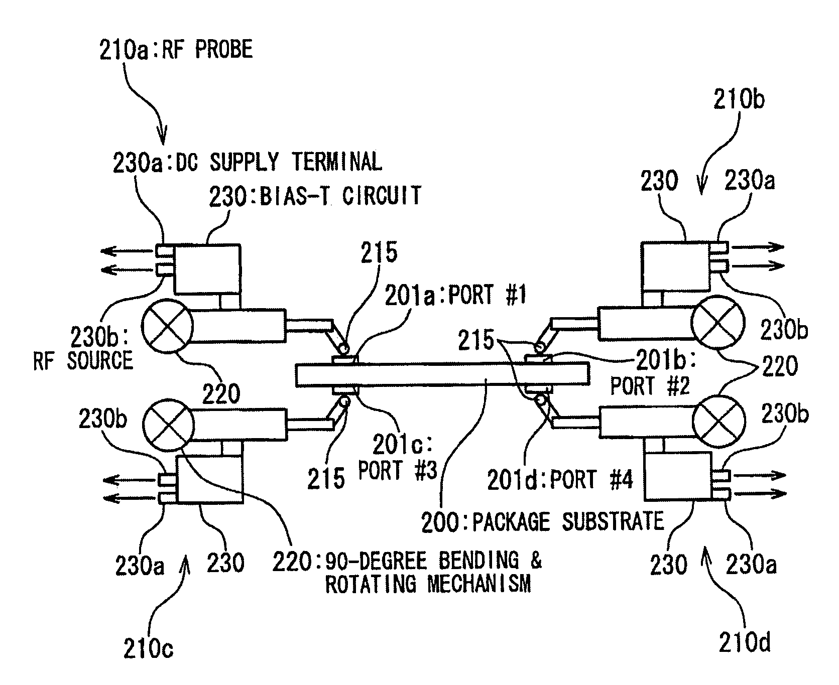
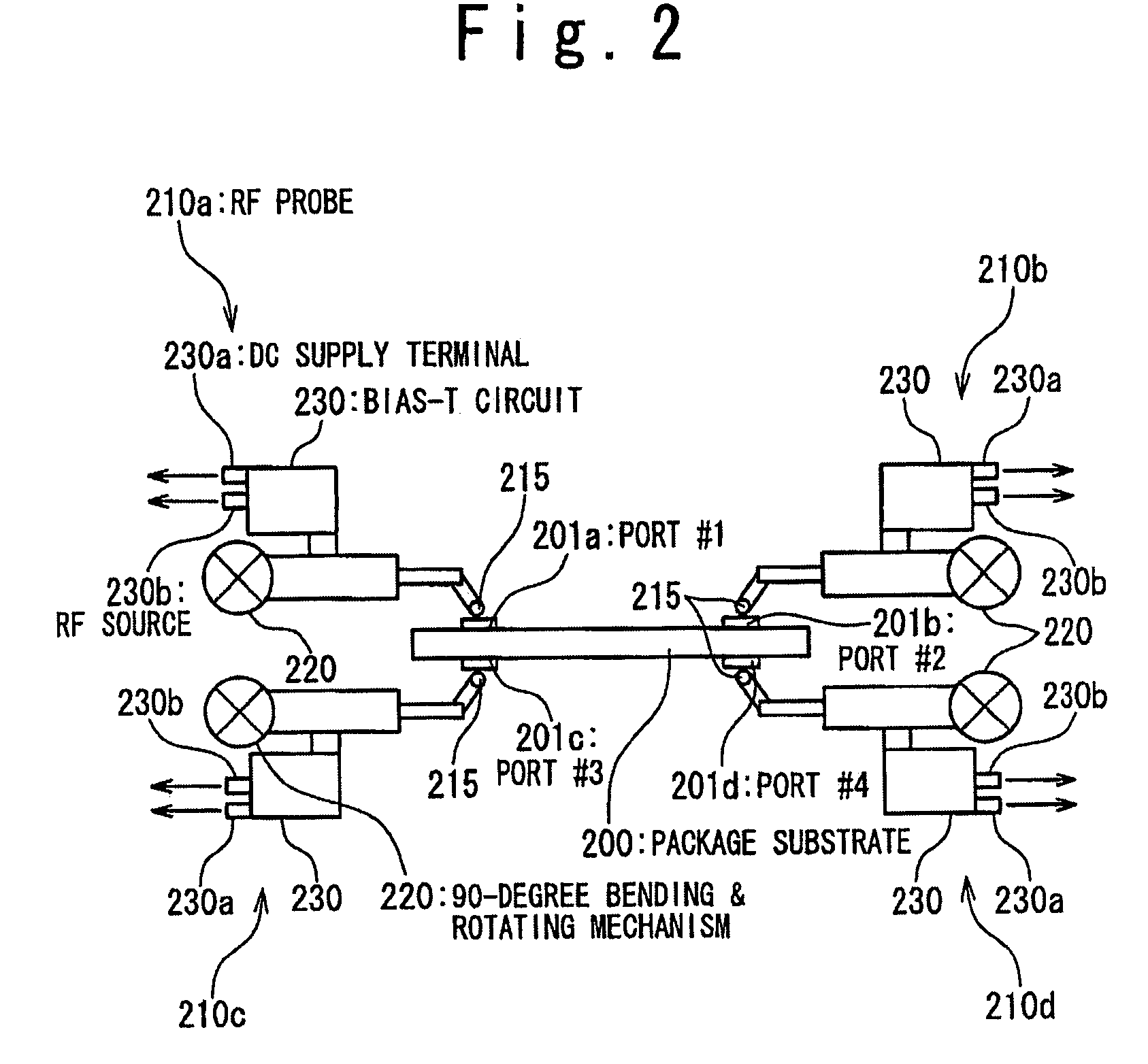
[0039]FIG. 2 is a cross sectional view schematically showing the structure of the impedance measuring apparatus according to the first embodiment of the present invention when a package substrate 200 as a measurement target is measured.

[0040]The impedance measuring apparatus in the first embodiment includes a processing unit (not shown) containing a network analyzer (not shown) and carrying out a calibration calculation, four RF (radio frequency) probes 210a to 210d, a 90-degree bending & rotating mechanism 220 connected to each of the RF probes 210a to 210d, a calibration substrate supporting mechanism 250 to support calibration substrates 240 (FIG. 3) in a horizontal or vertical state, and a mechanical controller (not shown). The mechanical controller (not shown) controls the rotation mechanisms 220 to be rotated.

[0041]Each of the RF probes 210a to 210d includes a DC supply terminal 230a, a Bias-T circuit 230 and a signal probe 215. The DC supply terminal 230a receives a DC voltag...

second embodiment

[0050]FIGS. 5 and 6 are diagram schematically showing the impedance measuring apparatus of the package substrate according to the second embodiment of the present invention. The basic configuration and operation principle of the impedance measuring apparatus in the second embodiment are the same as those in the first embodiment. However, a 180-degree bending & rotating mechanism 420 is provided in the second embodiment instead of the 90-degree bending & rotating mechanism 250.

[0051]The RF impedance measuring apparatus in the second embodiment includes two RF probes 410a and 410b, and the above-mentioned 180-degree bending & rotating mechanisms 420. Each of the RF probes 410a and 410b includes a DC supply terminal 430a to receive a DC bias, and a Bias-T circuit 430 to receive and combine the DC bias from the DC supply terminal 430a and an RF signal from the processing unit (not shown), and a signal probe 415. The Bias-T circuit 430 supplies the combined RF signal to a substrate throu...

third embodiment

[0056]FIG. 7 is a diagram schematically showing the RF impedance measuring apparatus of a package substrate according to the third embodiment of the present invention. The basic structure and measurement principles in the third embodiment are the same as those the second embodiment. However, the third embodiment includes scales for accurately measuring the position coordinates of RF probes 410a and 410b with respect to the three axis directions as shown in FIG. 7. Thus, the thickness (in Z direction) of the package substrate 400 and the distance between ports in within the same plane (XY plane) of the package substrate 400 can be accurately measured, thereby the phase correction can be carried out promptly and easily.

[0057]The RF impedance measuring apparatus of the third embodiment includes two RF probes 410a and 410b, two RF probe supporting mechanisms 450a and 450b to support the two RF probes 410a and 410b, and the 180-degree bending & rotating mechanism 420. As shown in FIG. 7,...


PUM


Abstract

An impedance measuring apparatus includes a plurality of RF (radio frequency) probes; a plurality of rotation mechanisms coupled to the plurality of RF probes, respectively; a processing unit, and a mechanical controller. The mechanical controller controls the plurality of rotation mechanisms and the plurality of RF probes to measure package RF signals between terminals formed on a package substrate. The processing unit measures calibration RF signals between terminals formed on at least one calibration substrate; determines RF impedances of the package substrate from the package RF signals and phase differences corresponding to a thickness of the package substrate and distances between the terminals on the package substrate from the calibration RF signals, and calibrates the RF impedances based on the phase differences.

Description

BACKGROUND OF THE INVENTION[0001]1. Field of the Invention[0002]The present invention relates to an apparatus and method for measuring RF (radio frequency) impedance of a semiconductor package substrate.[0003]2. Description of the Related Art[0004]Operation speed of a semiconductor device has been increasing rapidly in recent years, and high frequency characteristics of a semiconductor package substrate have been improved accordingly on which the semiconductor device is mounted. During this progress, a new unexpected problem is caused in the measurement of RF impedance (S-parameter) of the semiconductor package substrate at a test adjustment stage, because of the demand of higher characterization frequency for the semiconductor package substrate.[0005]FIG. 1 shows a conventional method for measuring the RF impedance (S-parameter) of a power source line in a package substrate 105. Referring to FIG. 1, a package substrate 105 is mounted on a substrate 110 such as a printed circuit boa...

Claims


Application Information

Patent Timeline
Patent Type & Authority Patents(United States)
IPC IPC(8): G01R27/08
CPCG01R31/2896
Inventor OIKAWA, RYUICHI
Owner RENESAS ELECTRONICS CORP
Learn More