Eureka AIR delivers breakthrough ideas for toughest innovation challenges, trusted by R&D personnel around the world.

Homoepitaxial gallium nitride based photodetector and method of producing

a photodetector and homoepitaxial technology, applied in the field ofcrystalline gallium nitride, can solve the problems of high dislocation, undesirable and detrimental effects, and inability to obtain high-quality gan substrates

Inactive Publication Date: 2007-11-06
SLT TECH
View PDF19 Cites 52 Cited by
  • Summary
  • Abstract
  • Description
  • Claims
  • Application Information

AI Technical Summary

Problems solved by technology

Because high-quality GaN substrates have not been available, virtually all of the art has involved heteroepitaxial deposition of GaN and GaInAlN on sapphire or SiC substrates.
The heteroepitaxial growth process often results in defects including high concentrations of dislocations, vacancies, or impurities.
These defects may have undesirable and detrimental effects on epitaxially grown gallium nitride, and may adversely influence operation of the resultant gallium nitride-based device.
These adverse influences include compromised electronic performance and operation.
Presently, heteroepitaxial gallium nitride growth processes require complex and tedious steps to reduce defect concentrations in the gallium nitride.
Known growth processes do not provide large gallium nitride crystals of high quality (i.e.; crystals having low dislocation densities); for example, gallium nitride crystals greater than about 0.8 inches (about 2 centimeters) in diameter or greater than about 0.01 inches (about 250 microns) in thickness.
Further, the known methods are not known to provide for production of large gallium nitride crystals that result in single-crystal gallium nitride boules, for example gallium nitride crystals of about 1 inch in diameter and about 0.5 inches in thickness, which are suitable for forming wafers.
Thus, applications for gallium nitride are limited due to size constraints.
As is the case in heteroepitaxial devices, high concentrations of such defects degrade device performance.
Also, most known gallium nitride crystal production processes do not provide high-quality gallium nitride crystals with low concentrations of impurities and dislocations with adequate size and growth rates that are acceptable for device applications.
Further, the known gallium nitride crystal production processes are not believed to provide an economical process having nitride growth rates that enable moderate-cost gallium nitride crystal production.
Therefore, applications for gallium nitride are further limited due to quality and cost-of-production factors.
Use of gallium nitride crystal has been limited in photodetector applications because of the quality and manufacturing issues discussed above.
While current buffer-layer technology allows for production of commercially viable GaN-based LEDs and LDs, the photodetectors that can be produced with current technology are marginal in performance because of very high defect levels.

Method used


Image

  • Homoepitaxial gallium nitride based photodetector and method of producing
  • Homoepitaxial gallium nitride based photodetector and method of producing
  • Homoepitaxial gallium nitride based photodetector and method of producing

Examples


Embodiment Construction

[0025]In the following detailed description, like reference characters designate like or corresponding parts throughout the several views shown in the figures. It is also understood that terms such as “top,”“bottom,”“outward,”“inward,” and the like are words of convenience and are not to be construed as limiting terms.

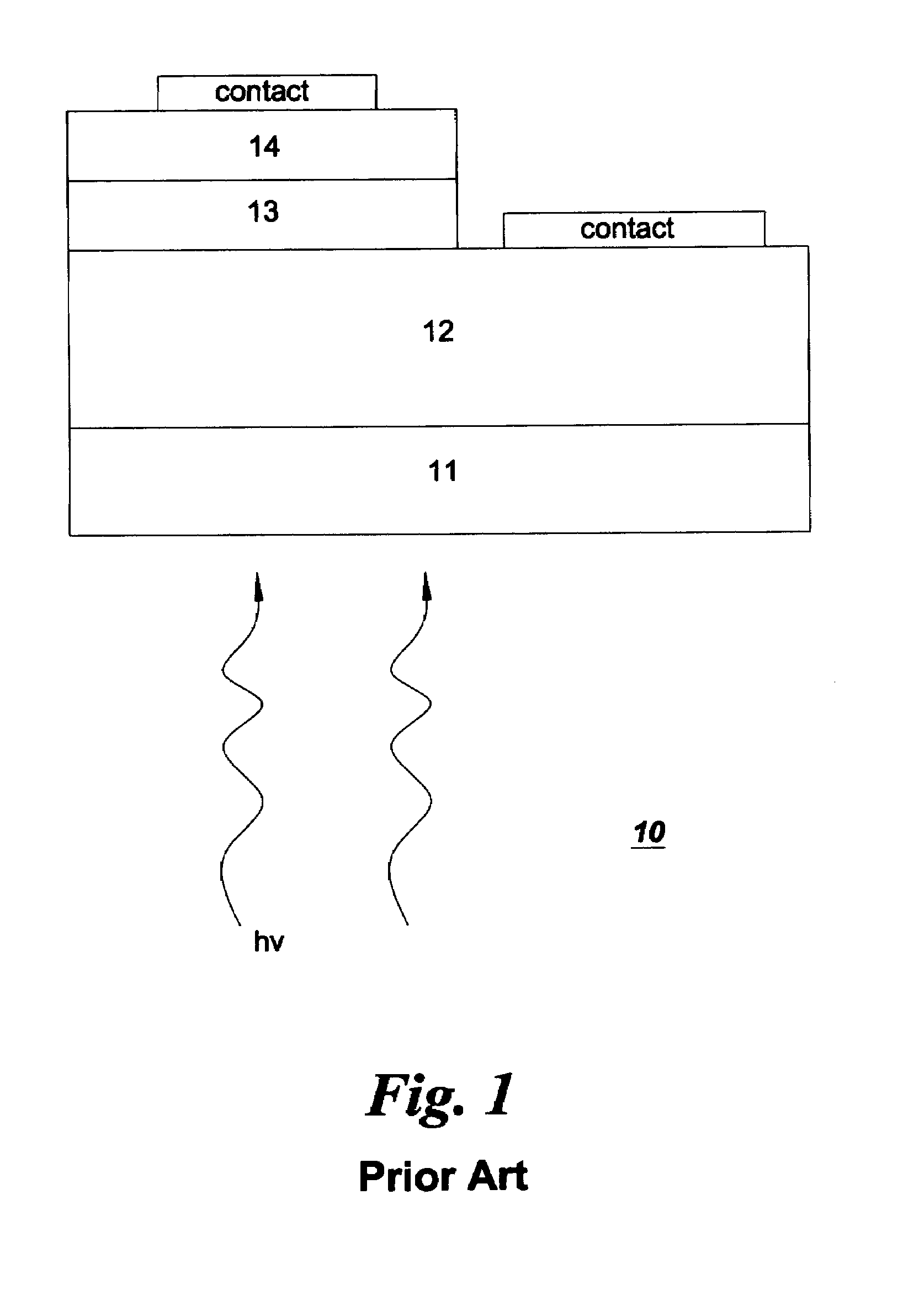
[0026]Referring to the drawings in general and to FIG. 1 in particular, it will be understood that the illustrations are for the purpose of describing a preferred embodiment of the invention and are not intended to limit the invention thereto. FIG. 1 depicts a prior art GaN / AlGaN on sapphire mesa p-i-n photodetector 10. Photodetector 10 comprises a sapphire substrate layer 11, an n-type AlGaN ohmic contact layer 12, an intrinsic GaN absorption layer 13, and a p-type GaN ohmic contact layer 14. The sapphire substrate layer 11 is transparent to the GaN absorption layers so it can detect the optical field from the backside. Layer 12 is comprises an n-type AlGaN layer and ...


PUM


Abstract

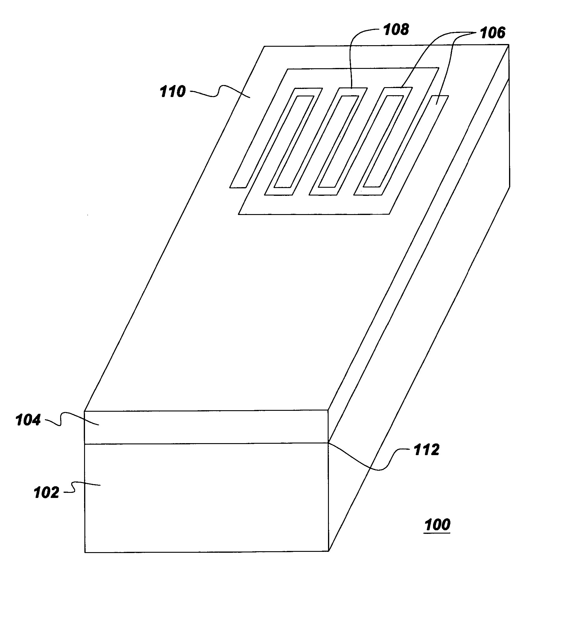
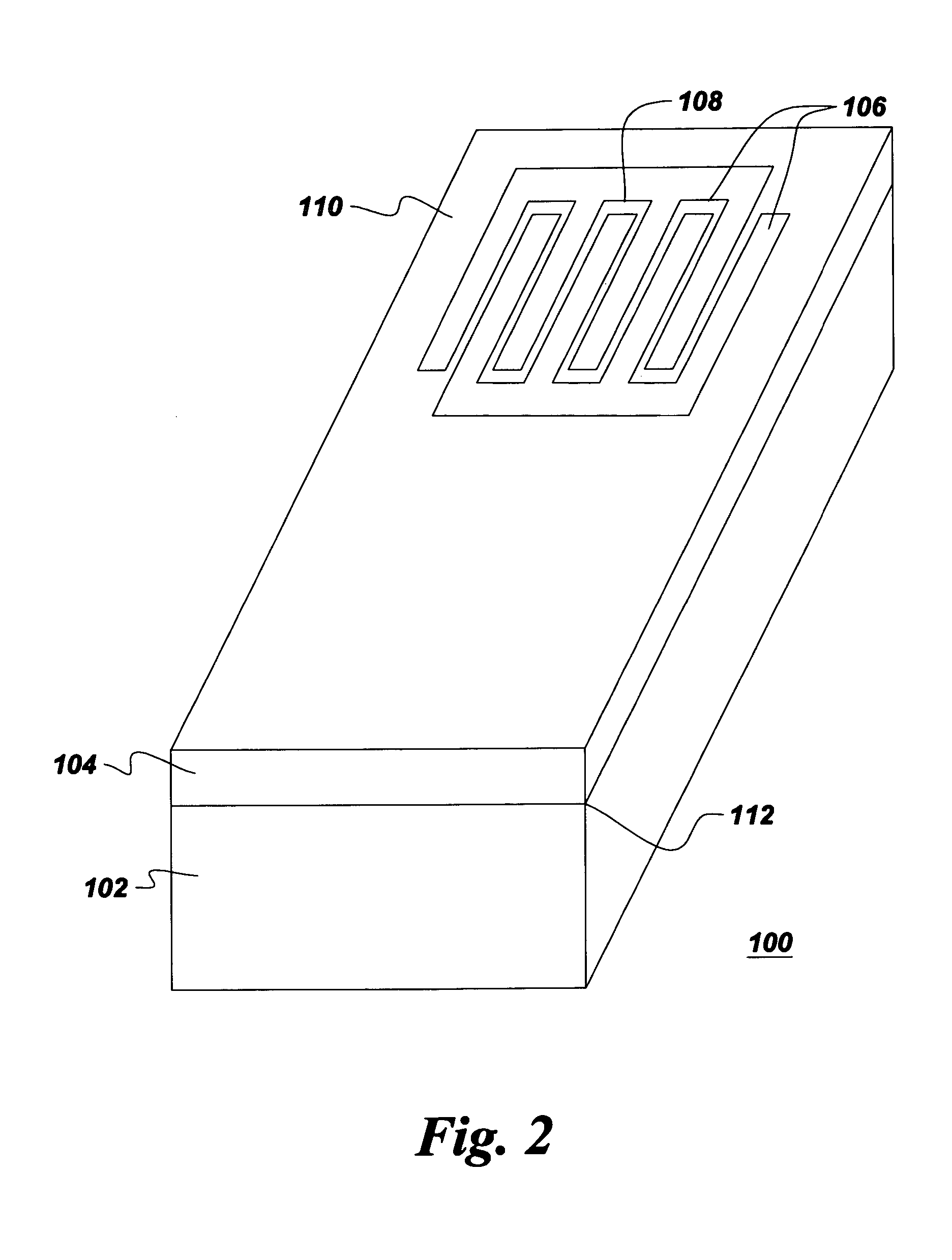
A photodetector (100, 200, 300) comprising a gallium nitride substrate, at least one active layer (104, 302) disposed on the substrate (102, 202, 306), and a conductive contact structure (106, 210, 308) affixed to the active layer (104, 302) and, in some embodiments, the substrate (102, 202, 306). The invention includes photodetectors (100, 200, 300) having metal-semiconductor-metal structures, P-i-N structures, and Schottky-barrier structures. The active layers (104, 302) may comprise Ga1-x-yAlxInyN1-z-w PzAsw, or, preferably, Ga1-xAlxN. The gallium nitride substrate comprises a single crystal gallium nitride wafer and has a dislocation density of less than about 105 cm−2. A method of making the photodetector (100, 200, 300) is also disclosed.

Description

CROSS-REFERENCE TO RELATED APPLICATIONS[0001]This application is a divisional of application Ser. No. 09 / 839,941, filed Apr. 20, 2001 now U.S. Pat. No. 6,806,508, which is hereby incorporated by reference in its entirety.BACKGROUND OF THE INVENTION[0002]The invention relates to crystalline gallium nitride. In particular, the invention relates to a homoepitaxial gallium nitride based photodetector and a method of producing the same.[0003]During the past decade there has been tremendous interest in gallium nitride (GaN) based optoelectronic devices, including, for example, light emitting diodes (LEDs) and laser diodes (LDs). Because high-quality GaN substrates have not been available, virtually all of the art has involved heteroepitaxial deposition of GaN and GaInAlN on sapphire or SiC substrates. A thin low-temperature buffer layer, typically AlN or GaN, is used in order to accommodate the lattice mismatch between GaN and the substrate and maintain an epitaxial relationship to the su...

Claims


Application Information

Patent Timeline
Patent Type & Authority Patents(United States)
IPC IPC(8): H01L21/20H01L31/0224H01L31/0304H01L31/108
CPCH01L31/022408H01L31/108H01L31/0304Y02E10/544Y02P70/50
Inventor D'EVELYN, MARK PHILIPEVERS, NICOLE ANDREACHU, KANIN
Owner SLT TECH
Why Eureka
Eureka Blog
Learn More