
Electro-optical device, image printing apparatus, and method of manufacturing electro-optical device

a technology of electrooptical devices and image printing, applied in the direction of separation processes, instruments, filtration separation, etc., can solve the problems of deteriorating light use efficiency, difficult to arrange the adhesive before hardening in only necessary portions, and difficult to arrange the adhesive before hardening. to achieve the effect of reducing light loss

Inactive Publication Date: 2007-09-25
SEIKO EPSON CORP
View PDF16 Cites 15 Cited by
  • Summary
  • Abstract
  • Description
  • Claims
  • Application Information

AI Technical Summary

Benefits of technology

This configuration enhances the light usage efficiency by ensuring more light is focused on the converging lens array, allowing for improved image formation and potentially extending the lifespan of the light-emitting elements by reducing the required voltage.

Problems solved by technology

That is, this structure has a problem in that the usage efficiency of light is deteriorated.
It is difficult to arrange the adhesive before hardened in only necessary portions of the receiving hole since the adhesive has fluidity.
It is difficult to arrange the adhesive before hardened in only necessary portions of the spacer unit since the adhesive has fluidity.

Method used


Image

  • Electro-optical device, image printing apparatus, and method of manufacturing electro-optical device
  • Electro-optical device, image printing apparatus, and method of manufacturing electro-optical device
  • Electro-optical device, image printing apparatus, and method of manufacturing electro-optical device

Examples


Embodiment Construction

Structure of Electro-optical Device

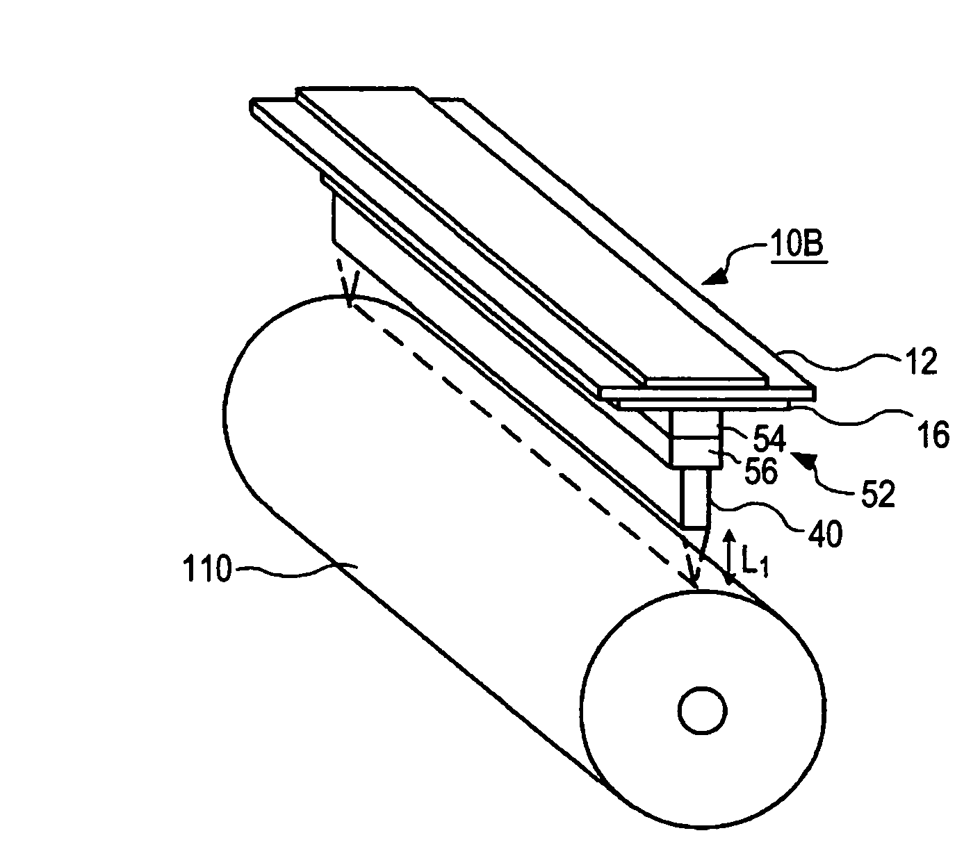
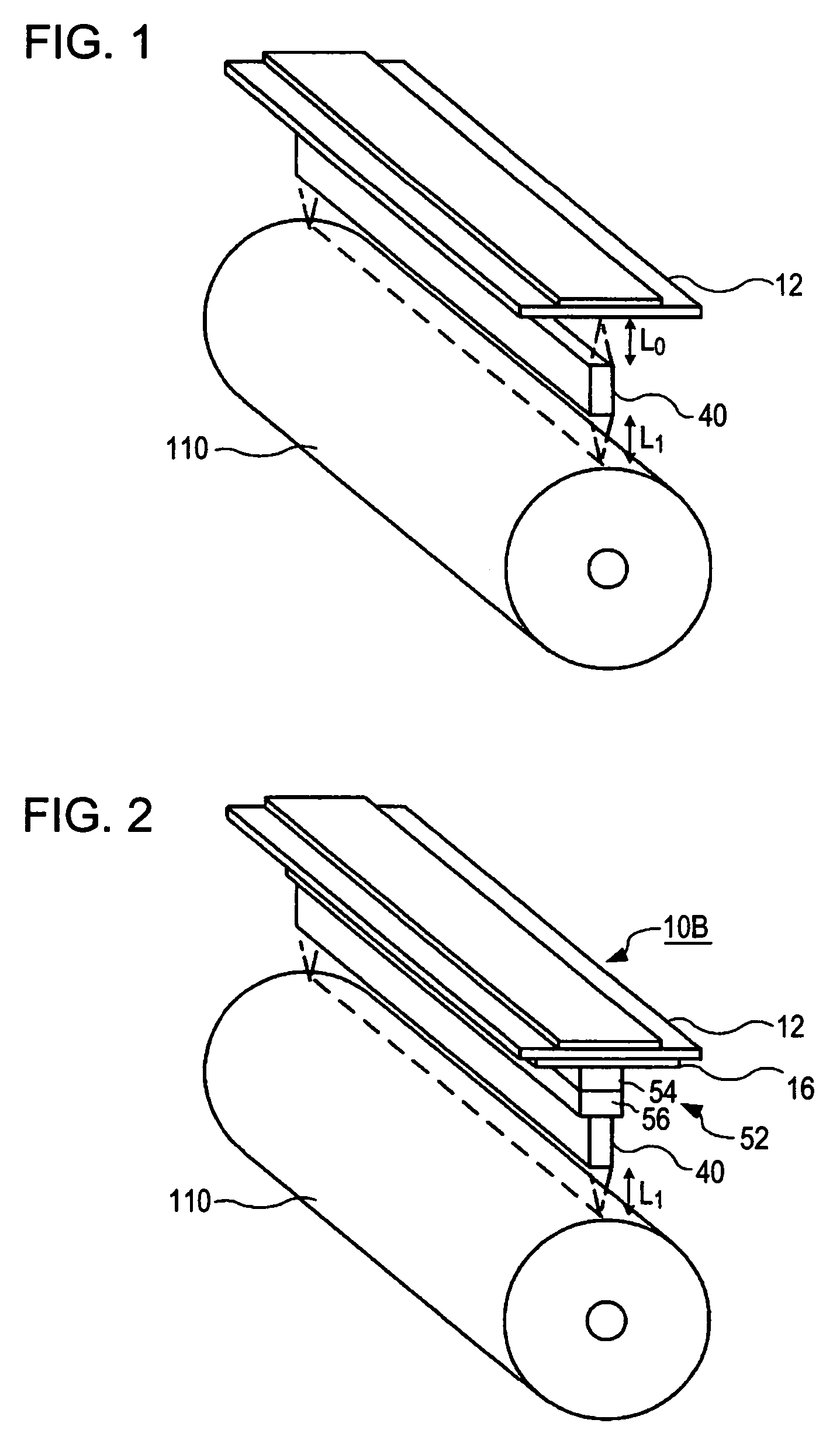
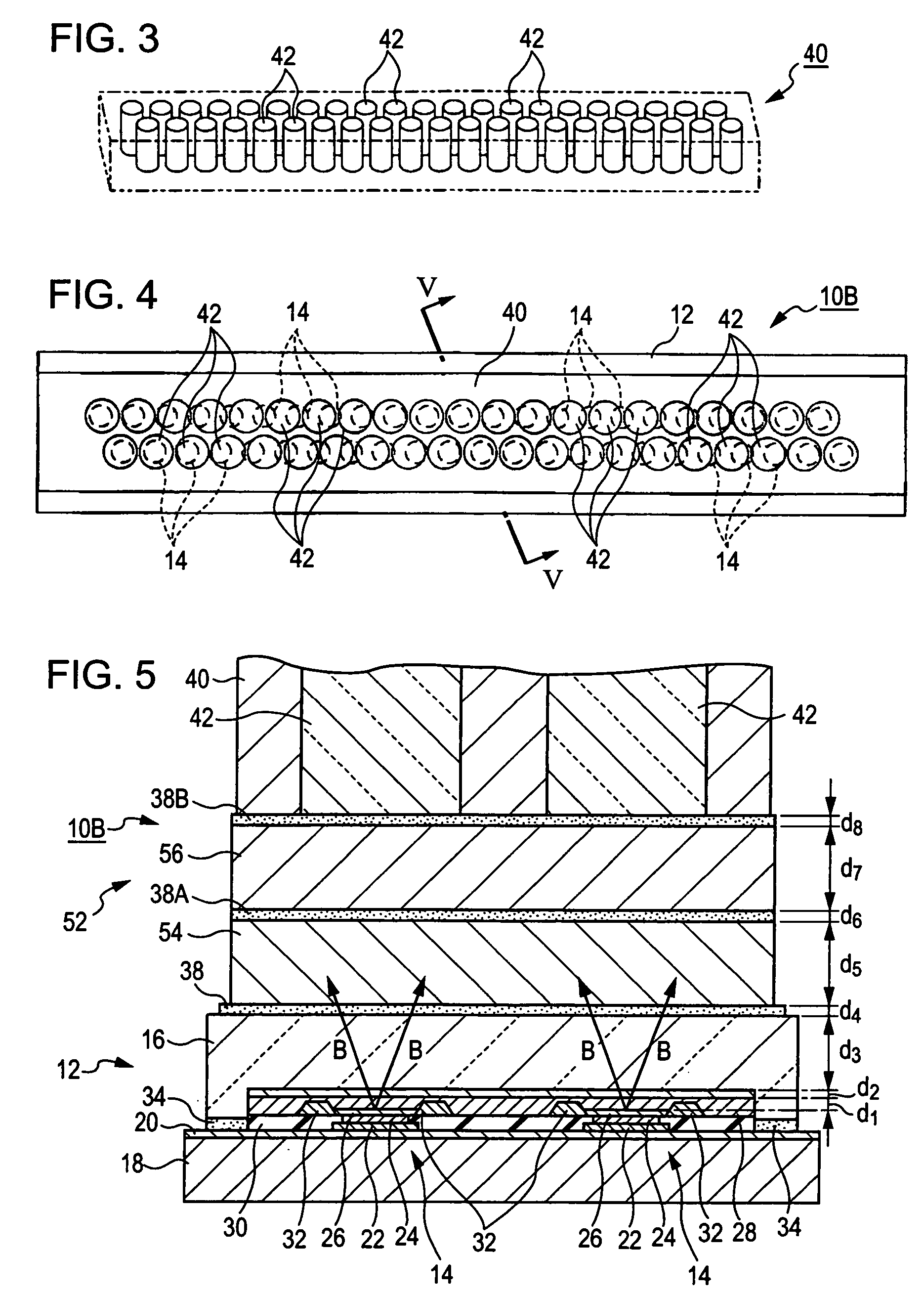
[0058]FIG. 2 is a perspective view schematically illustrating an electro-optical device 10B according to an embodiment of the invention. The electro-optical device 10B shown in FIG. 2 is used as a linear optical head for writing a latent image on an image carrier (for example, a photosensitive drum 110 shown in FIG. 2) in an image printing apparatus using an electrophotography method. The electro-optical device 10B includes a light-emitting panel (an electro-optical panel) 12 having a plurality of organic EL elements (electro-optical elements) arranged on the same surface and a conversing lens array 40 overlapping the light-emitting panel 12. A transmissive spacer unit 52 formed of, for example, glass or plastic is interposed between the light-emitting panel 12 and the converging lens array 40, and the spacer unit 52 has a plurality of laminated transmissive spacer members 56 and 58. The converging lens array 40 is arranged between the light-emitti...


PUM

PropertyMeasurementUnit
refractive indexaaaaaaaaaa

Abstract

An electro-optical device includes an electro-optical panel which has a plurality of electro-optical elements whose light-emitting characteristics or transmissive characteristics are changed by electrical energy applied; a converging lens array which has a plurality of distributed index lenses, each transmitting light traveling in the electro-optical panel to form an erect image with respect to an image on the electro-optical panel, the images formed by the plurality of distributed index lenses constituting a continuous image; and a transmissive spacer unit which is provided between the electro-optical panel and the converging lens array so as to be bonded to them. The spacer unit includes a laminated structure of a plurality of transmissive spacer members.

Description

BACKGROUND[0001]1. Technical Field[0002]The present invention relates to an electro-optical device provided with an electro-optical panel having electro-optical elements, such as light-emitting elements or light valve elements, therein, to an image printing apparatus using an electro-optical device, and to a method of manufacturing an electro-optical device.[0003]2. Related Art[0004]There has been developed a technique for using an electro-luminescent element (hereinafter, referred to as ‘EL elements’) array to write an electrostatic latent image on an image carrier (for example, a photosensitive drum) of an image printing apparatus using an electrophotography method. In this technique, generally, a converging lens array is provided between the EL element array and the image carrier (for example, see JP-A-63-103288 and JP-A-2004-58448 (FIG. 7)). For example, SLA (SELFOC lens array) available from Nippon Sheet Glass Co., Ltd. is used as an example of the conversing lens array (SELFOC...

Claims


Application Information

Patent Timeline
Patent Type & Authority Patents(United States)
IPC IPC(8): G02B3/00B41J15/14B41J27/00G02B27/10
CPCB41J2/451G02F1/133526G02B3/0006G02B3/0056B01D35/1573C02F1/4618
Inventor UEMATSU, KOICHI
Owner SEIKO EPSON CORP
Learn More