
Integrated MIS photosensitive device using continuous films

a photosensitive device and continuous film technology, applied in the field of image sensors, can solve the problems of low signal level of mesa-isolated mis and p-i-n photodiode sensors, disadvantages of conventional photosensitive devices, and poor image signals of isolating mis and p-i-n photodiodes

Inactive Publication Date: 2007-04-24
VAREX IMAGING CORP
View PDF10 Cites 15 Cited by
  • Summary
  • Abstract
  • Description
  • Claims
  • Application Information

AI Technical Summary

Benefits of technology

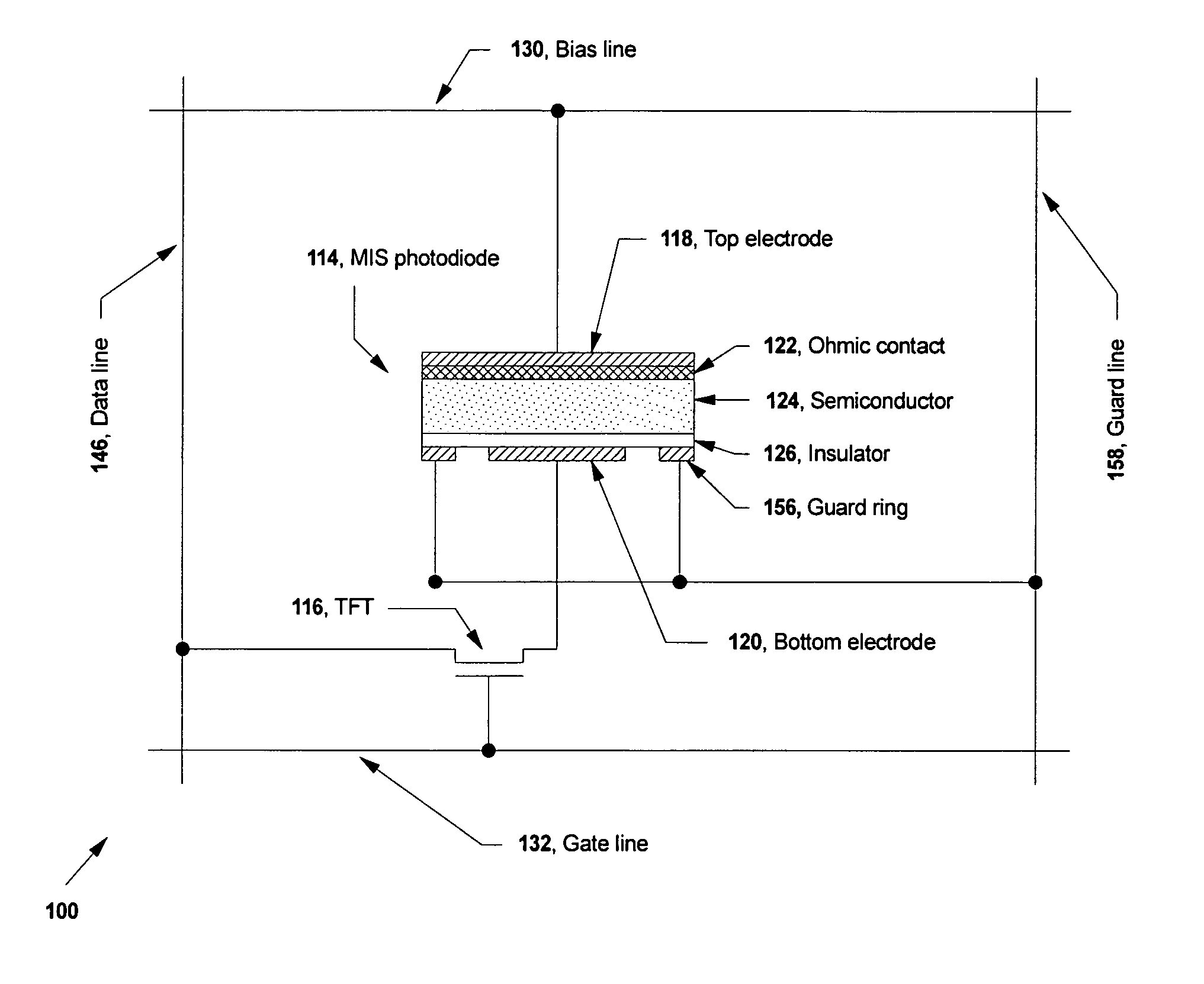
[0050]In another embodiment of the presently claimed invention which may prove advantageous, additional dielectric layers are incorporated between the dielectric layer 126 and the semiconductor layer 124 (see FIGS. 4, 6–7, 9, 11–12 and 14). The dielectric material between the bottom electrodes 120 and the continuous semiconductor layer 124 must serve several purposes. This dielectric material must have sufficient thickness and structural integrity to not breakdown under the electric fields established between the bottom electrodes 120 and the continuous top electrode 118. This dielectric material must be sufficiently free of internal stresses so as to not warp the underlying substrate 12. This dielectric material must also form an interface with the continuous semiconductor layer 124 which minimizes electron and hole trap states (trap states lead to image lag problems; i.e., ghost images). It may be that no one continuous dielectric layer 126 can adequately satisfy all these requirements.

Problems solved by technology

However, such conventional photosensitive devices have disadvantages.
Both the mesa-isolated MIS and p-i-n photodiodes typically generate poor image signals.
As noted above, a disadvantage common to mesa-isolated MIS and p-i-n photodiode sensors is low signal levels.
Accordingly, maximum possible signal strength cannot be achieved.
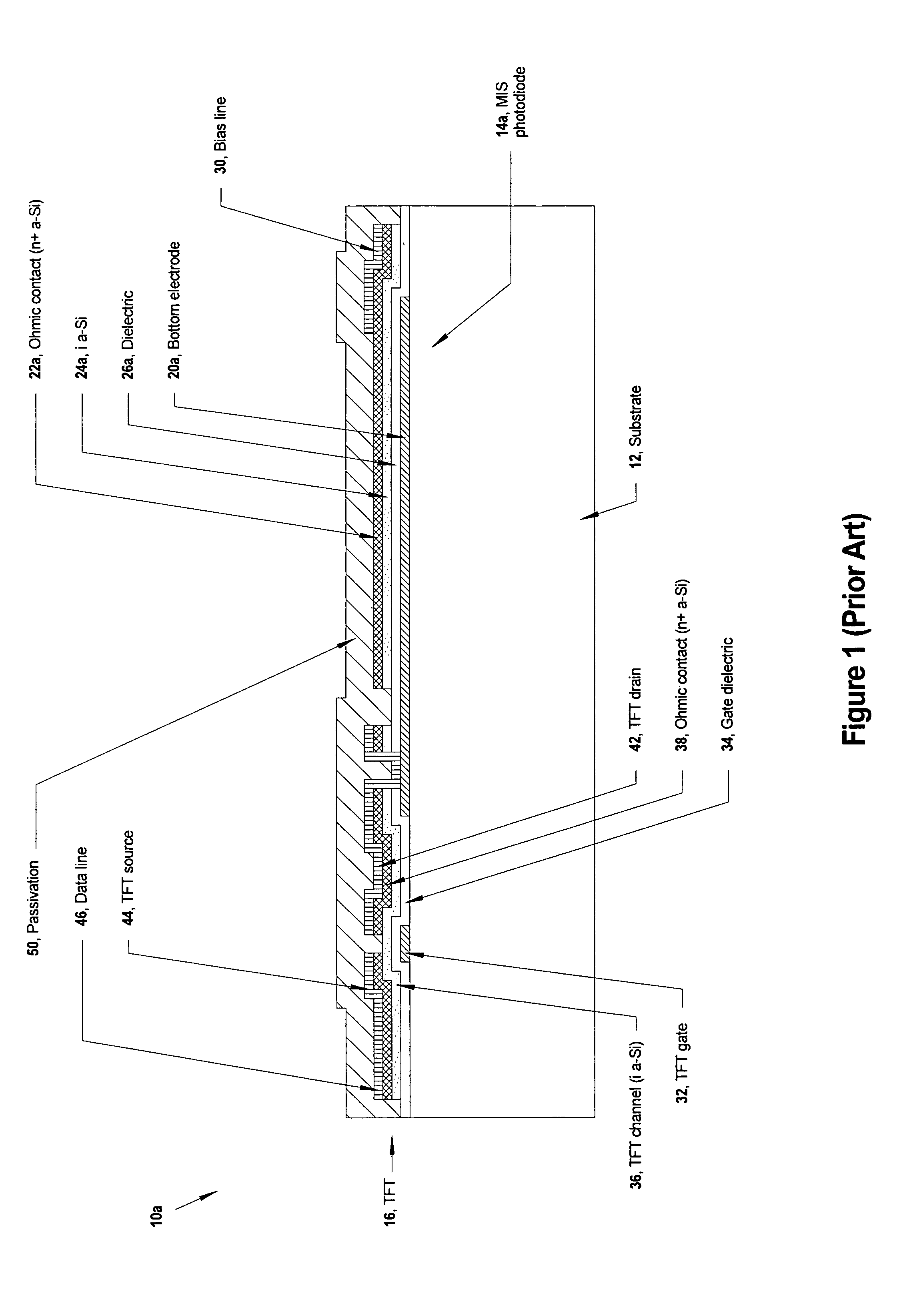
The mesa-isolated MIS photodiode structure of FIG. 1 has a further disadvantage.
However, this structure can suffer from significant crosstalk between adjacent pixels.

Method used


Image

  • Integrated MIS photosensitive device using continuous films
  • Integrated MIS photosensitive device using continuous films
  • Integrated MIS photosensitive device using continuous films

Examples


Embodiment Construction

[0029]The following detailed description is of example embodiments of the presently claimed invention with references to the accompanying drawings. Such description is intended to be illustrative and not limiting with respect to the scope of the present invention. Such embodiments are described in sufficient detail to enable one of ordinary skill in the art to practice the subject invention, and it will be understood that other embodiments may be practiced with some variations without departing from the spirit or scope of the subject invention.

[0030]Referring to FIG. 4, a pixel circuit 100 in accordance with one embodiment of the presently claimed invention includes the MIS photodiode 114 and a TFT 116 connected to a bias line 130, gate line 132 and data line 146, all in accordance with well known pixel circuit techniques. The MIS photodiode 114 includes an optically transparent top electrode 118 and a bottom electrode 120, between which are the semiconductor layers 122, 124 and ins...


PUM


Abstract

An integrated photosensitive device with a metal-insulator-semiconductor (MIS) photodiode constructed with one or more substantially continuous layers of semiconductor material and with a substantially continuous layer of dielectric material.

Description

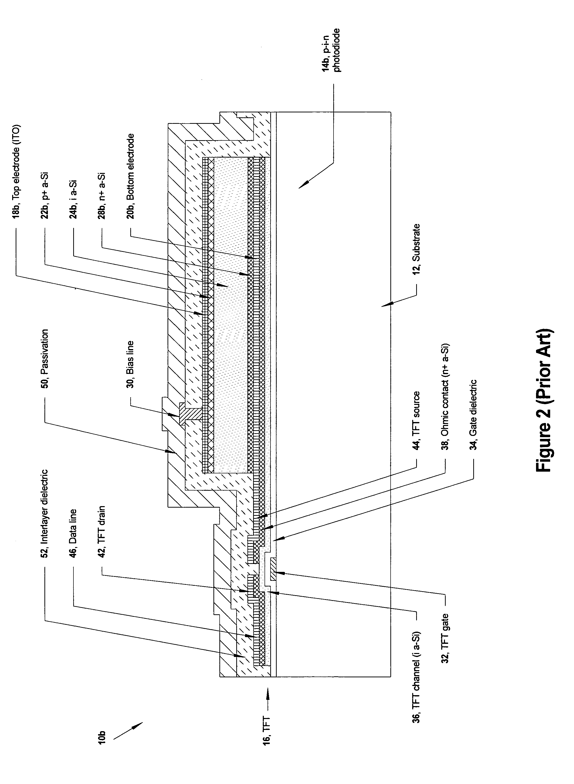
BACKGROUND OF THE INVENTION[0001]1. Field of the Invention[0002]The present invention relates to image sensors, and in particular, to image sensors with pixel circuits implemented with metal-insulator-semiconductor (MIS) photodiodes.[0003]2. Description of the Related Art[0004]Image sensors, such as those used for large area X-ray imaging, often use pixel circuits in which a mesa-isolated MIS photodiode is used as the photosensitive device. (A mesa-isolated device is formed by etching away a portion of the active materials, leaving a “mesa” of active materials.) Another common photosensitive device is a mesa-isolated p-i-n photodiode. Yet another conventional photosensitive device is a p-i-n photodiode comprised substantially of continuous films. However, such conventional photosensitive devices have disadvantages. Both the mesa-isolated MIS and p-i-n photodiodes typically generate poor image signals. The p-i-n photodiode comprised substantially of continuous films exhibits signific...

Claims


Application Information

Patent Timeline
Patent Type & Authority Patents(United States)
IPC IPC(8): H01L31/00
CPCH01L27/1463H01L27/14632H01L31/1133H01L31/12
Inventor WRIGHT, MICHAEL DEAN
Owner VAREX IMAGING CORP
Learn More