Photogate for use in an imaging device
a technology of photogate and imaging device, which is applied in the field of cmos imager, can solve the problems of high power dissipation of large arrays, ccd imagers also suffer from a number, and are susceptible to radiation damage, so as to improve the quantum efficiency of the photosensor and improve the short wavelength light response
- Summary
- Abstract
- Description
- Claims
- Application Information
AI Technical Summary
Benefits of technology
Problems solved by technology
Method used
Image
Examples
first embodiment
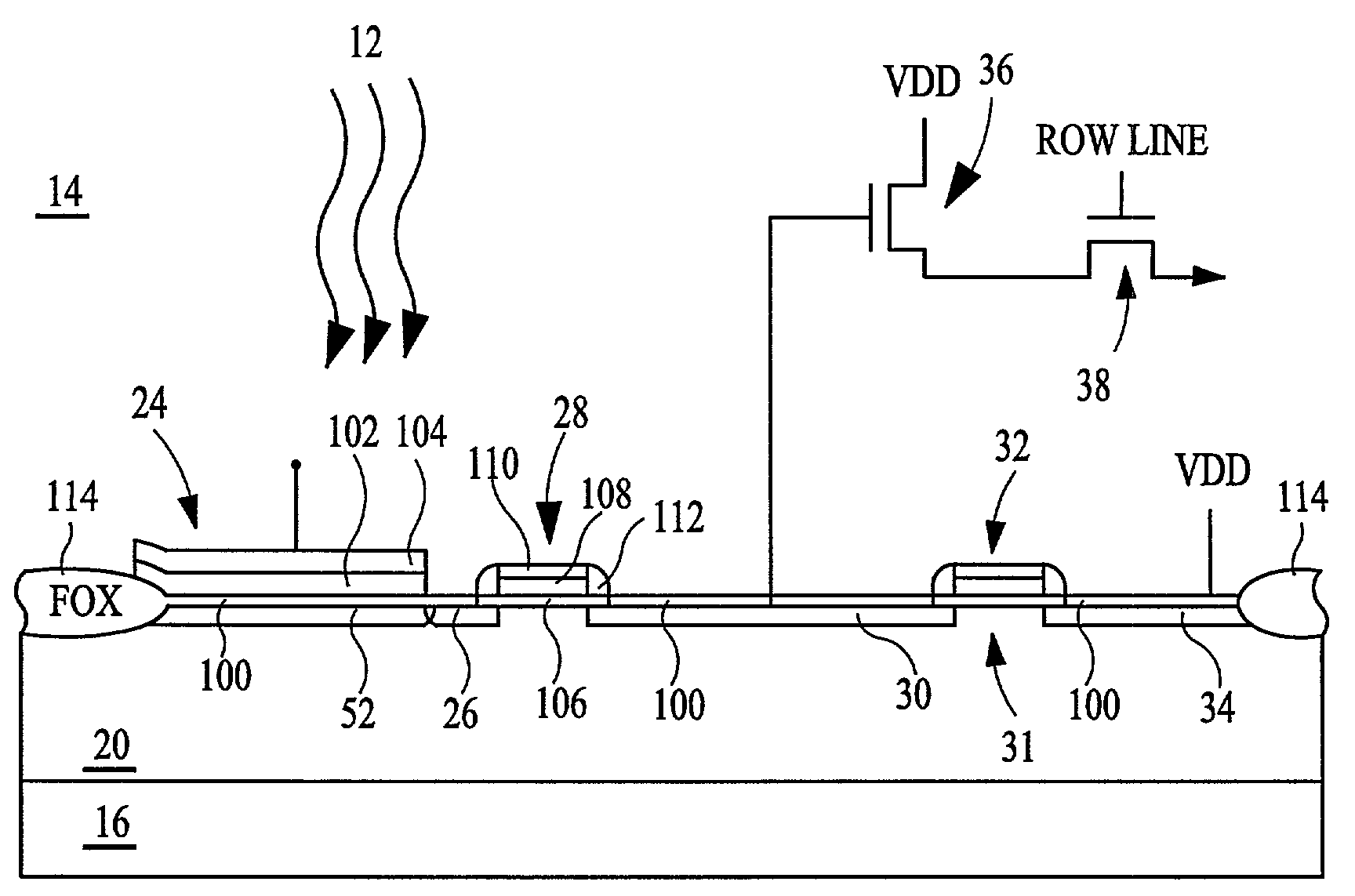
[0047]The structure of the pixel cell 14 of the first embodiment is shown in more detail in FIGS. 5 and 6. The pixel 14 may be formed in a substrate 16 having a doped layer or well 20 of a first conductivity type, which for exemplary purposes is treated as p-type. The doped layer 20 is provided with four doped regions 52, 26, 30, 34 formed therein, which are doped to a second conductivity type, which for exemplary purposes is treated as n-type. The first doped region 52 underlies the photogate 24, which comprises a thin layer 102 of doped silicon material transparent to radiant energy 12, such as doped polysilicon. The thin layer 102 is approximately 50 to 1500 Angstroms thick, and preferably has a thickness within the range of 50 to 800 Angstroms, and most preferably is 300 Angstroms thick.
[0048]A gate oxide layer 100 of silicon dioxide is formed between the thin layer 102 and the doped layer 20. Insulating sidewalls 112 of silicon dioxide (oxide), silicon nitride (nitride), silico...
second embodiment
[0060]The pixel cell 14 of the second embodiment requires further processing steps to form the photogate 24, as shown in FIG. 13. The top conductive layer 104 is formed by CVD or sputtering, or other suitable means, depending on the material of the layer 104. The layer 104 may be any transparent conductive material, such as indium tin oxide, indium oxide, tin oxide, or the like. The top conductive layer 104 is very thin, i.e., the thickness is within the range of 100 to 3000 Angstroms. After deposition of the layer 104, the layers 102 and 104 are patterned to form a stacked photogate 24. Conventional processing methods may then be used to form contacts and wiring to connect gate lines and other connections in the pixel cell 14, as described above.
[0061]The pixel cell 14 of the third embodiment is formed in a fashion similar to that of the first embodiment. After the pixel cell 14 has been processed up through the gate oxide formation depicted in FIG. 11, the next step is to form the...
PUM
 Abstract
Description
Claims
Application Information
 - R&D
- Intellectual Property
- Life Sciences
- Materials
- Tech Scout
- Unparalleled Data Quality
- Higher Quality Content
- 60% Fewer Hallucinations
Browse by: Latest US Patents, China's latest patents, Technical Efficacy Thesaurus, Application Domain, Technology Topic, Popular Technical Reports.
© 2025 PatSnap. All rights reserved.Legal|Privacy policy|Modern Slavery Act Transparency Statement|Sitemap|About US| Contact US: help@patsnap.com


