Electronically controllable arrayed waveguide gratings
a waveguide and array technology, applied in the field of arrayed waveguide gratings, can solve the problems of “phase errors, very expensive temperature controlled chips, and adversely affecting the performance of the awg
- Summary
- Abstract
- Description
- Claims
- Application Information
AI Technical Summary
Benefits of technology
Problems solved by technology
Method used
Image
Examples
Embodiment Construction
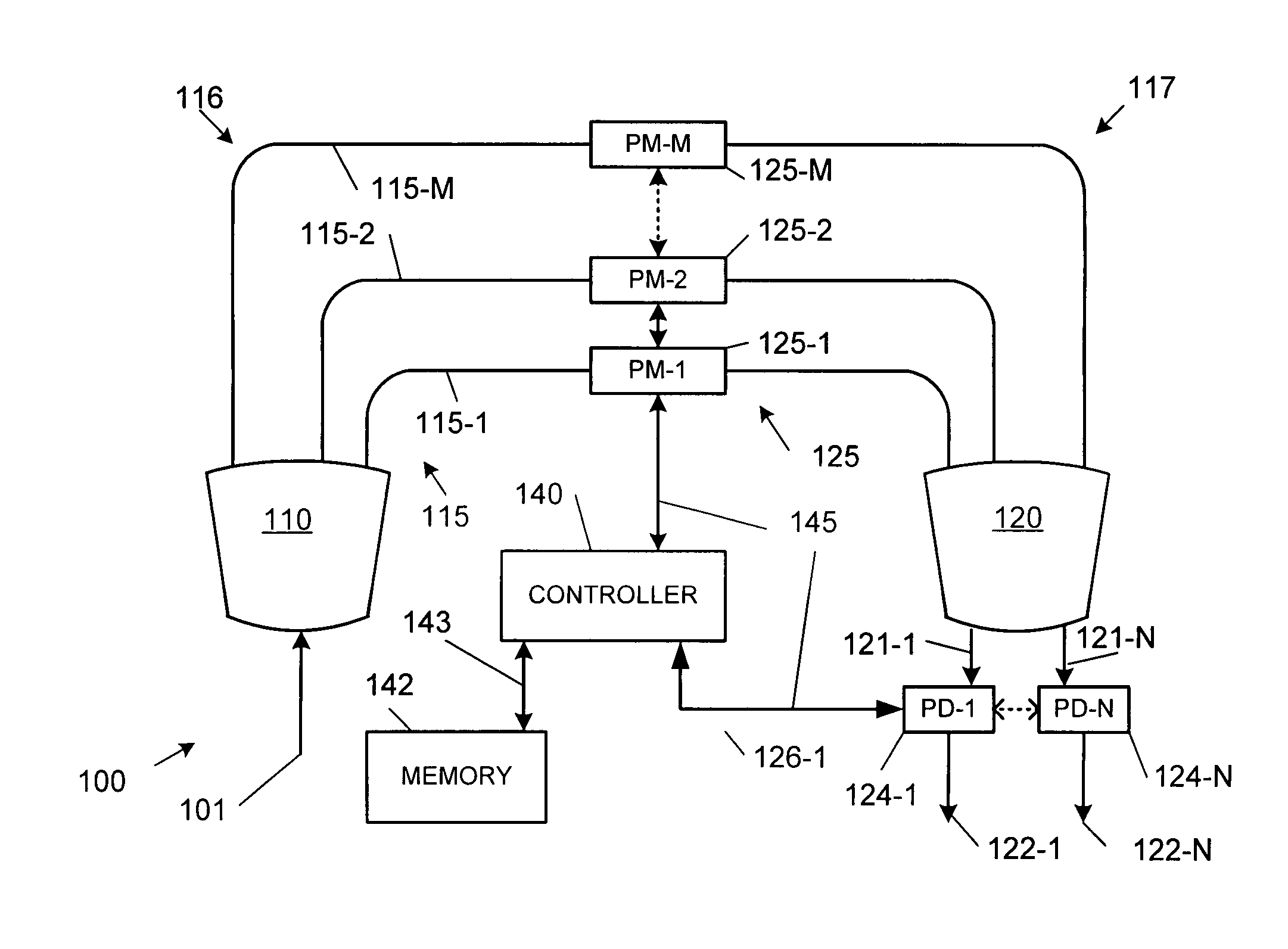
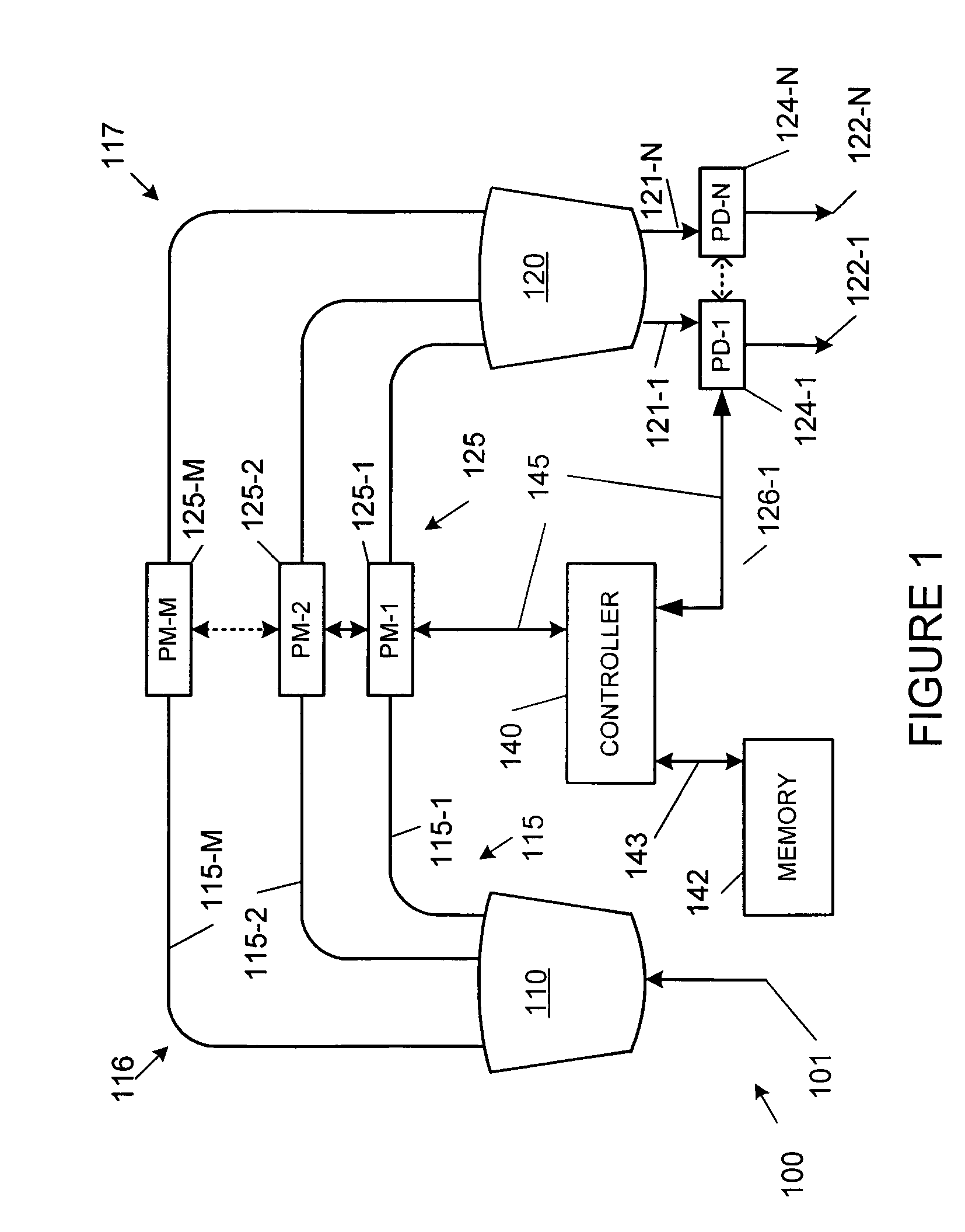
[0017]FIG. 1 is a diagram of an integrated electronically controllable arrayed waveguide grating (AWG), configures as a demultiplexer, with adjustable phase modulators, according to one embodiment of the present invention. AWG 100 has optical input 101 and optical outputs 122. AWG 100 includes input slab 110, arrayed waveguides 115, photodetectors 124, phase modulators 125 and output slab 120. There are M arrayed waveguides 115 connected between input slab 110 and output slab 120. There can be many, as in dozens or even hundreds of arrayed waveguides 115, such as 115-1, 115-2 and 115-M in an AWG. Only three are shown in FIG. 1 to simplify the diagram. The number of arrayed waveguides 115 is dependent on the specific design and application of the AWG. AWG 100 is a demultiplexer with a multiplexed input 101 and demultiplexed outputs 122-1 to 122-N, where N is the number of channels processed by AWG 100.
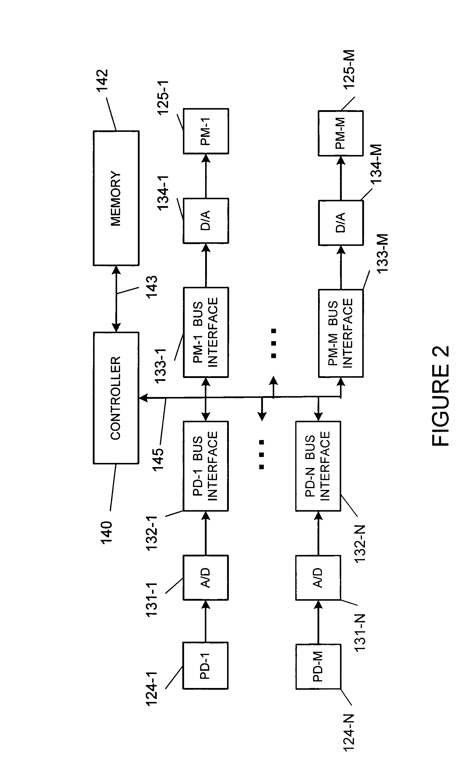
[0018]Controller 140 is connected to bus 145, which operates as a control and data ...
PUM
 Abstract
Description
Claims
Application Information
 - R&D
- Intellectual Property
- Life Sciences
- Materials
- Tech Scout
- Unparalleled Data Quality
- Higher Quality Content
- 60% Fewer Hallucinations
Browse by: Latest US Patents, China's latest patents, Technical Efficacy Thesaurus, Application Domain, Technology Topic, Popular Technical Reports.
© 2025 PatSnap. All rights reserved.Legal|Privacy policy|Modern Slavery Act Transparency Statement|Sitemap|About US| Contact US: help@patsnap.com


