LSI test socket for BGA
a test socket and lsi technology, applied in the direction of electrical testing, measurement devices, instruments, etc., can solve the problems of significantly serious problems, high power current, and high running costs, and achieve stable operation test, improved manufacturing stability and test stability, and reduced power supply fluctuation of lsi operating at high frequencies
- Summary
- Abstract
- Description
- Claims
- Application Information
AI Technical Summary
Benefits of technology
Problems solved by technology
Method used
Image
Examples
first embodiment
(First Embodiment)
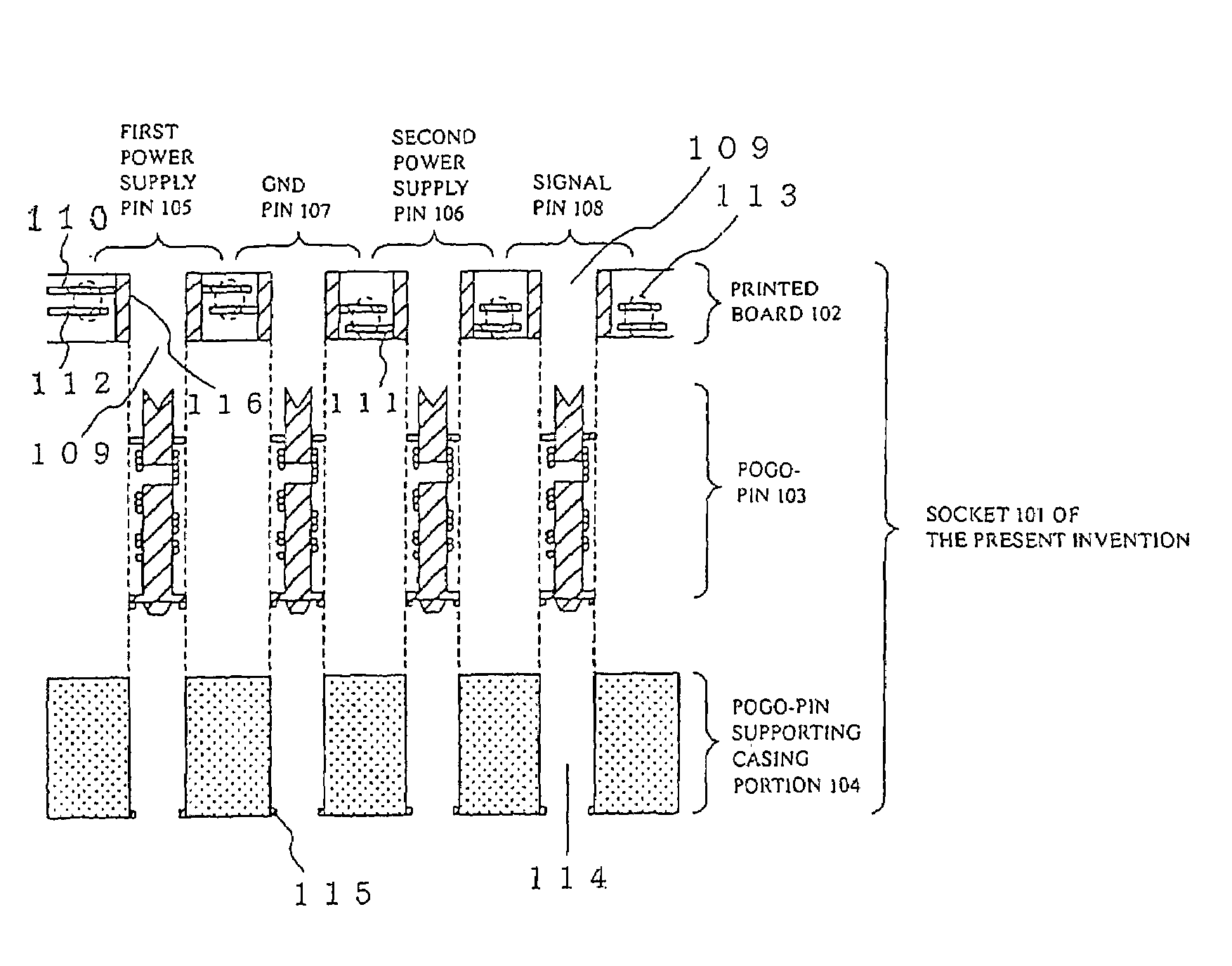
[0029]A first embodiment of the present invention will be described below. FIG. 4 is an exploded longitudinal sectional view showing each component comprising an LSI socket for BGA in accordance with the present invention. FIG. 5 is a longitudinal sectional view showing an LSI socket for BGA illustrating the first embodiment in accordance with the present invention.
[0030]As shown in FIG. 4, an LSI socket 101 in accordance with the present invention is composed of three components: a printed board 102, pogo-pins 103, and a pogo-pin supporting casing portion 104. The printed board 102 is provided with a plurality of through holes 109 into which a first power supply pin 105 and a second power supply pin 106 in which voltage values to be applied are different, a GND pin 107, and the pogo-pins 103 coming into use for a signal pin 108 are each inserted, plating layers 116 being formed in inner surfaces of all the through holes 109 other than the through hole 109 through ...
second embodiment
(Second Embodiment)
[0035]Next, a second embodiment of the present invention will be described with reference to the drawings. FIG. 6 is an exploded longitudinal sectional view showing each component comprising an LSI socket for BGA in accordance with the second embodiment. FIG. 7 is a longitudinal sectional view showing the LSI socket for BGA in accordance with the second embodiment.
[0036]As shown in FIG. 6, an LSI socket 201 in accordance with the present invention is composed of four components: pogo-pin lower portion components 203A, a printed board 202, pogo-pin upper portion components 203B, and a pogo-pin supporting casing portion 204. The printed board 202 is provided with a plurality of through holes 209 into which a first power supply pin 205 and a second power supply pin 206 in which voltage values to be applied are different, a GND pin 207, and pogo-pins 203 (consisting of 203A and 203B) coming into use for a signal pin 208 are each inserted, plating layers 216 being form...
PUM
 Abstract
Description
Claims
Application Information
 - R&D
- Intellectual Property
- Life Sciences
- Materials
- Tech Scout
- Unparalleled Data Quality
- Higher Quality Content
- 60% Fewer Hallucinations
Browse by: Latest US Patents, China's latest patents, Technical Efficacy Thesaurus, Application Domain, Technology Topic, Popular Technical Reports.
© 2025 PatSnap. All rights reserved.Legal|Privacy policy|Modern Slavery Act Transparency Statement|Sitemap|About US| Contact US: help@patsnap.com


