Robot end effector position error correction using auto-teach methodology

a robot arm and robot arm technology, applied in the field of specimen handling robots, can solve the problems of scratches, wafer damage to the wafer and contamination of the other wafers, and achieve the effect of reducing specimen damag

Active Publication Date: 2006-05-02
BOOKS AUTOMATION US LLC
View PDF9 Cites 30 Cited by
  • Summary
  • Abstract
  • Description
  • Claims
  • Application Information

AI Technical Summary

Benefits of technology

[0008]An object of this invention is, therefore, to provide a specimen handling device that minimizes specimen damage and the production of contaminate particles.
[0009]Another object of this invention is to provide a semiconductor wafer handling device that can quickly and accurately transfer semiconductor wafers between a wafer cassette and a wafer processing station.
[0012]The end effectors are generally spatula-shaped and have a proximal end that is operably connected to a robot arm. The active contact point is located at the proximal end, which allows the end effector to be lighter, stronger, and more slender than end effectors having moving mechanisms that may not fit between adjacent wafers in a cassette. The lack of moving mechanisms further causes the end effector to produce less contamination within the cassette. Additionally, locating the active contact point at the proximal end of the end effector ensures that it is remote from harsh conditions such as heated environments and liquids.
[0014]Alternative embodiments of the end effector include flat or inclined, narrow or arcuate rest pads onto which the wafer is initially loaded. The narrow and arcuate inclined rest pad embodiments assist in centering and gripping the wafer between the active contact point and the distal rest pads. The arcuate rest pads more readily accommodate gripping and handling flatted wafers.
[0015]The end effectors further include fiber optic light transmission sensors for accurately locating the wafer edge and bottom surface. The sensors provide robot arm extension, elevation, and positioning data that support methods of rapidly and accurately placing a wafer on and retrieving a wafer from a wafer transport stage or a process chamber, and placing a wafer in and retrieving a wafer from among a stack of closely spaced wafers stored in a wafer cassette. The methods include position error sensing and correction for effectively preventing accidental contact between the end effector and adjacent wafers stacked in a cassette.

Problems solved by technology

Unfortunately, positioning errors while transferring the wafer among the cassette, robot arm, and processing stations, such as a prealigner, may cause damage to the wafer and contamination of the other wafers in the cassette because intentional engagement as well as inadvertent touching of the wafer may dislodge particles that can fall and settle onto the other wafers.
Wafer damage can include scratches as well as metallic and organic contamination of the wafer material.

Method used


Image

  • Robot end effector position error correction using auto-teach methodology
  • Robot end effector position error correction using auto-teach methodology
  • Robot end effector position error correction using auto-teach methodology

Examples


first embodiment

[0034]FIGS. 1 and 2 show a spatula-shaped end effector 10 of this invention for transferring semiconductor wafers, such as a wafer 12 (shown transparent to reveal underlying structures), to and from a wafer cassette 14. End effector 10 is adapted to receive and securely hold wafer 12 and transfer it to and from cassette 14 for processing. FIG. 2 shows that end effector 10 is particularly adapted for retrieving and replacing wafer 12 from among closely spaced wafers, such as wafers 12, 12A, and 12B, which are shown as they might be stacked in wafer cassette 14. Wafers having diameters of less than 150 mm are typically spaced apart at a 4.76 mm ( 3 / 16 inch) pitch distance; 200 mm diameter wafers are typically spaced apart at a 6.35 mm (¼ inch) pitch distance; and 300 mm wafers are typically spaced apart at a 10 mm (0.394 inch) pitch distance.

[0035]End effector 10 is operably attached to a robot arm 16 (a portion of which is shown) that is programmably positionable in a well known mann...

second embodiment

[0050]FIGS. 5 and 6 show a spatula-shaped end effector 110 of this invention for transferring semiconductor wafers, such as wafer 12 (shown transparent to reveal underlying structures), to and from wafer cassette 14 (not shown in this view). End effector 110 is similar to end effector 10 but is further adapted to sense the bottom surface of a wafer stored in wafer cassette 14 without protruding into the cassette. FIG. 6 shows that end effector 110 is particularly adapted for retrieving and replacing wafer 12 from among closely spaced apart wafers, such as wafers 12, 12A, and 12B, which are shown as they might be stacked in wafer cassette 14.

[0051]End effector 110 is operably attached to robot arm 16. In general, end effector 110 senses the bottom surface of wafer 12 before entering wafer cassette 14 to retrieve wafer 12 from between wafers 12 A and 12B. End effector 110 is then finely positioned by robot arm 16 and actuated to grip periphery 18 of wafer 12, remove wafer 12 from cass...

third embodiment

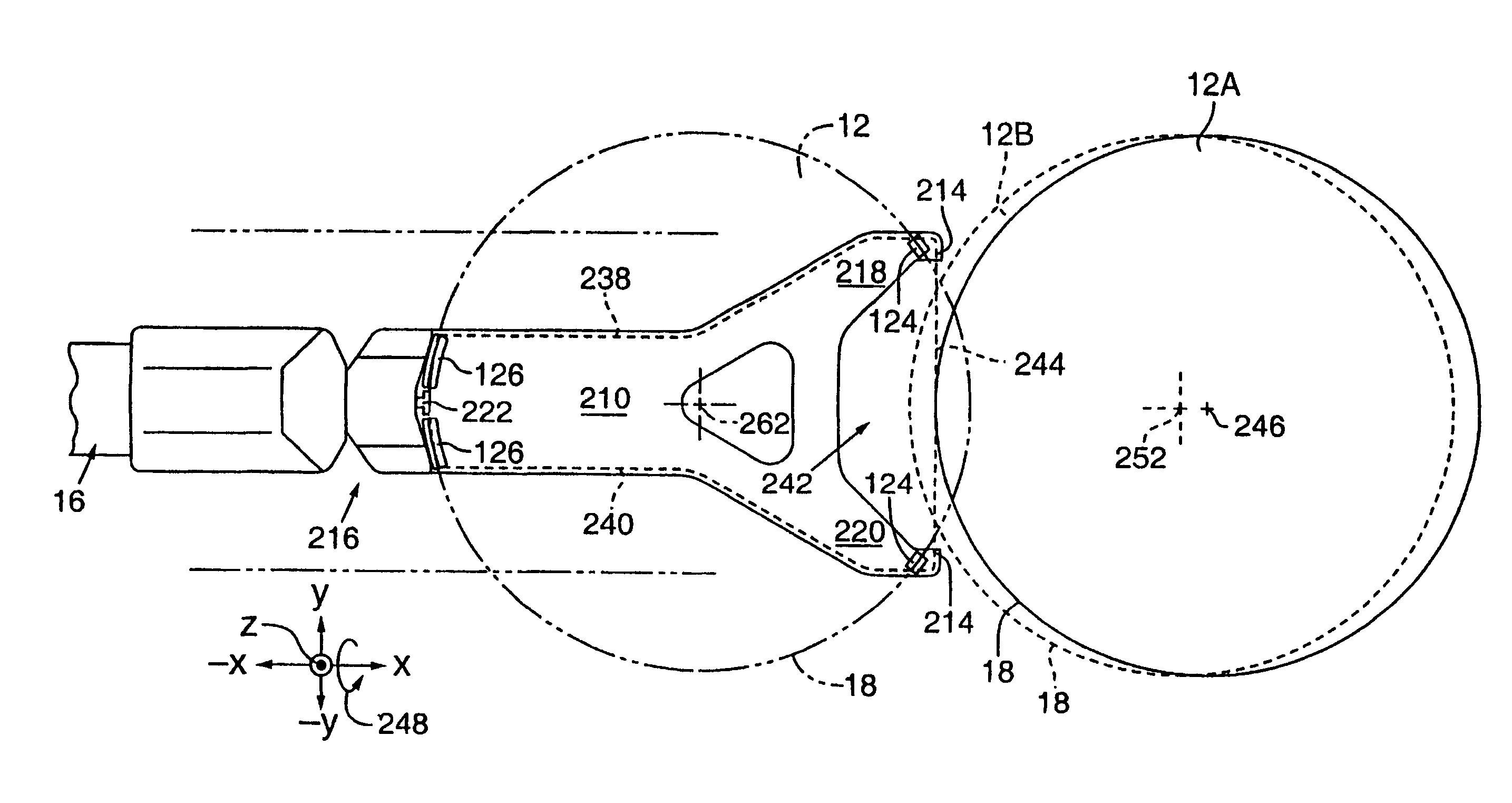
[0082]FIGS. 10, 11, and 12 show a preferred fork-shaped end effector 210 of this invention for transferring semiconductor wafers, such as wafer 12 (shown transparent to reveal underlying structures), to and from wafer cassette 14 (not shown in these views). End effector 210 is similar to end effectors 10 and 110 but includes a position sensing active contact point actuating mechanism 212 and distal end sensors 214 to accomplish various wafer sensing measurements.

[0083]FIG. 11 shows that end effector 210 is particularly suited for retrieving and replacing wafer 12 from among closely spaced apart wafers, such as wafers 12, 12A, and 12B, which are shown as they might be stacked in wafer cassette 14.

[0084]FIG. 12 shows end effector 210 operably coupled to robot arm 16 at a proximal end 216 and extending to forked distal ends 218 and 220. End effector 210 receives wafer 12 between proximal end 216 and forked distal ends 218 and 220 and preferably includes at least two and, more preferabl...


PUM


Abstract

A robot arm positioning error is corrected by employing a specimen gripping end effector in which a light source and a light receiver form a light transmission pathway that senses proximity to the specimen. A robot arm old position is sensed and recorded. The robot arm retrieves the specimen from the old position and employs old position information to replace the specimen at a new position that is ideally the same as the old position. A robot arm new position is sensed and recorded. A difference between the new and old positions represents a position error. A correct position is obtained by processing the position error and the old position information.

Description

RELATED APPLICATIONS[0001]Not ApplicableFEDERALLY SPONSORED RESEARCH OR DEVELOPMENT[0002]Not ApplicableTECHNICAL FIELD[0003]This invention relates to specimen handling robots, and more particularly, to an edge gripping semiconductor wafer robot arm end effector positioning error reducing method.BACKGROUND OF THE INVENTION[0004]Integrated circuits are produced from wafers of semiconductor material. The wafers are typically housed in a cassette having a plurality of closely spaced slots, each of which can contain a wafer. The cassette is typically moved to a processing station where the wafers are removed from the cassette, placed in a predetermined orientation by a prealigner or otherwise processed, and returned to another location for further processing.[0005]Various types of wafer handling devices are known for transporting the wafers to and from the cassette and among processing stations. Many employ a robotic arm having a spatula-shaped end that is inserted into the cassette to r...

Claims


Application Information

Patent Timeline
Patent Type & Authority Patents(United States)
IPC IPC(8): G06F19/00
CPCB25J9/1692B25J19/025H01L21/67259H01L21/681H01L21/68707H01L21/67742Y10T74/20317
Inventor BACCHI, PAULFILIPSKI, PAUL S.
Owner BOOKS AUTOMATION US LLC
Why Eureka
Try Eureka