Method and apparatus for assembling electronics

a technology of electronics and a method, applied in the field of apparatus and a method for assembling electronics, can solve the problems of affecting the quality of electronics,

Inactive Publication Date: 2005-08-09
EXATRON
View PDF7 Cites 5 Cited by
  • Summary
  • Abstract
  • Description
  • Claims
  • Application Information

AI Technical Summary

Problems solved by technology

These dedicated mechanisms are expensive, typically costing hundreds of thousands of dollars each; moreover, a separate mechanism has to be provided for each separate programmer, so that the total cost equals the cost of one dedicated mechanism multiplied by the total number of programmers.
These dedicated mechanisms also take up a large amount of space that can be used, for example, by more feed devices.
They also inhibit throughput, because they tend to be slow.

Method used


Image

  • Method and apparatus for assembling electronics
  • Method and apparatus for assembling electronics
  • Method and apparatus for assembling electronics

Examples


Embodiment Construction

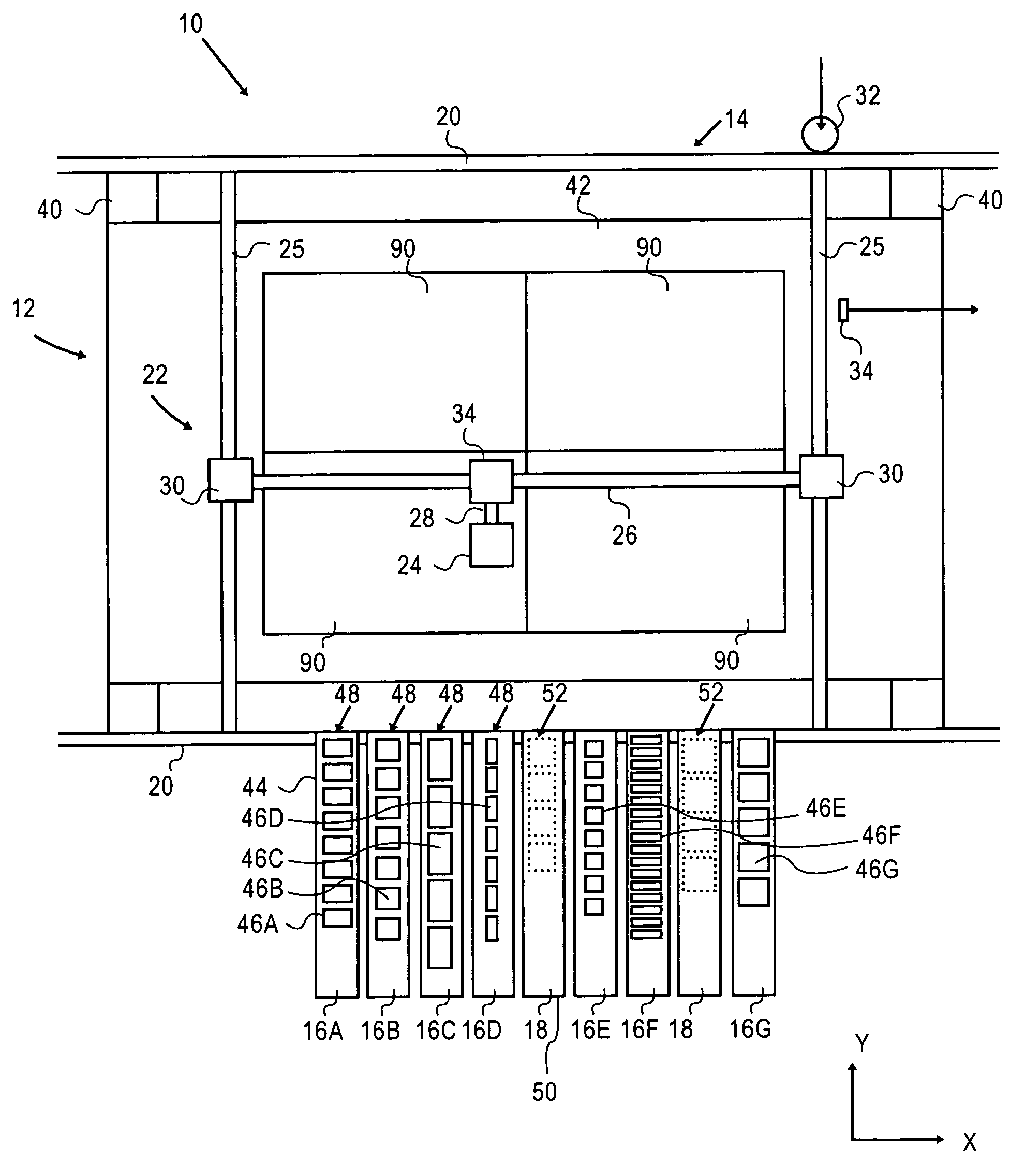
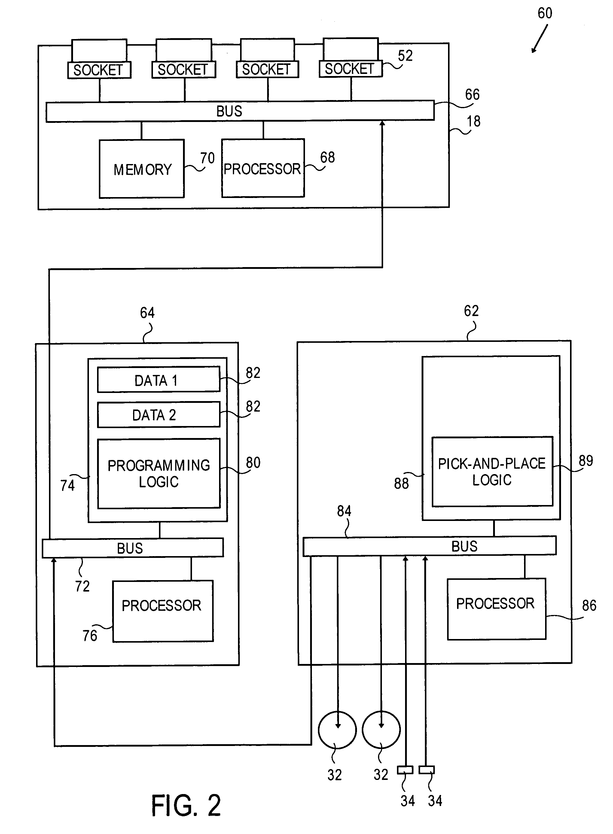
[0019]FIG. 1 of the accompanying drawings illustrates an apparatus 10 for assembling electronics, according to an embodiment of the invention. The apparatus 10 includes a transport system 12, a pick-and-place system 14, feed devices 16, and programmers 18 (or testers, in another embodiment). Essentially, the apparatus 10 utilizes the pick-and-place system 14 to transfer electronic devices held by the feed devices 16 to circuit boards on the transport system 12, and also utilizes the pick-and-place system 14 to transfer some of these electronic devices to and from the programmers 18. This provides a faster and less expensive alternative than when a separate mechanism is used for transferring devices from feed devices to separate programmers and back from the programmers to the feed devices.

[0020]Specifically, the pick-and-place system 14 includes a support frame 20, a pick-and-place mechanism 22, and a device-engaging component 24. The pick-and-place mechanism 22 includes two y-rails...


PUM

PropertyMeasurementUnit
timeaaaaaaaaaa
areaaaaaaaaaaa
electricalaaaaaaaaaa

Abstract

An apparatus for assembling electronics is provided, comprising a support frame, at least one pick-and-place mechanism, at least one device-engaging component, a feed device, and a programmer or tester. The pick-and-place mechanism is secured to the support frame. The device-engaging component is secured to the pick-and-place mechanism. The feed device has a slender body secured to the frame to feed a plurality of electronic devices to a feed location. The programmer or tester has a slender body secured to the support frame in a side-by-side relationship relative to the feed device. The programmer or tester has a socket located at an intermediate location. The devices are movable by the device-engaging component from the feed location to the socket at the intermediate location.

Description

BACKGROUND OF THE INVENTION[0001]1). Field of the Invention[0002]This invention relates generally to an apparatus and a method for assembling electronics, more specifically to programming or testing of the electronics.[0003]2). Discussion of Related Art[0004]Electronic assemblies such as printed circuit boards, etc., are usually manufactured by transferring a circuit board to an assembly area and then using a pick-and-place device to transfer individual electronic components from separate, adjacent feed devices such as tape feeders or cartridge feeders to the circuit board. The circuit board, with the electronic devices thereon, is then transferred through a reflow oven, whereafter the electronic devices are secured to the circuit board.[0005]It is often necessary to program some of these electronic devices before they are located on the circuit board. The electronic devices are usually separately programmed before being located in or on tapes, cartridges, etc. In some cases a mecha...

Claims


Application Information

Patent Timeline
Patent Type & Authority Patents(United States)
IPC IPC(8): H05K3/30H05K13/04
CPCH05K13/0417Y10T29/53178Y10T29/53261Y10T29/4913Y10T29/49133H05K13/082
Inventor HOWELL, ROBERT P.
Owner EXATRON
Why Eureka
Try Eureka