Line-shaped antenna
a line-shaped antenna and antenna technology, applied in the structural form of radiating elements, waveguide devices, resonance antennas, etc., can solve the problems of resonance frequency rise, corresponding portion is easily deformed, narrowed bandwidth of meander antennas, etc., and achieves stable antenna properties and easy deformation
- Summary
- Abstract
- Description
- Claims
- Application Information
AI Technical Summary
Benefits of technology
Problems solved by technology
Method used
Image
Examples
trial example 1
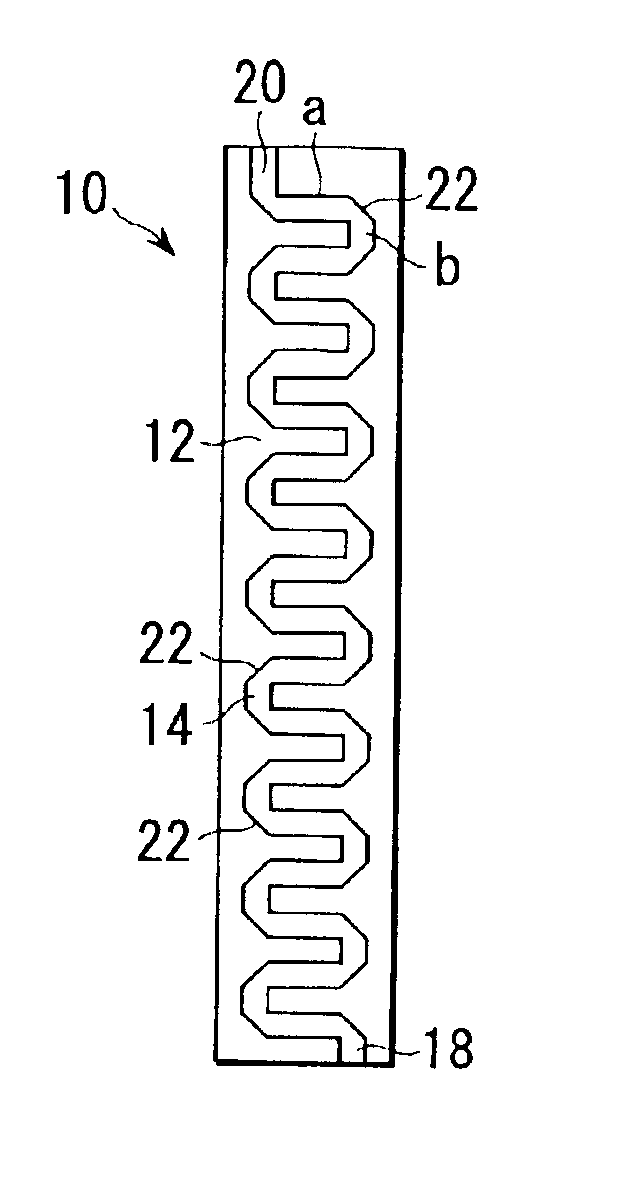
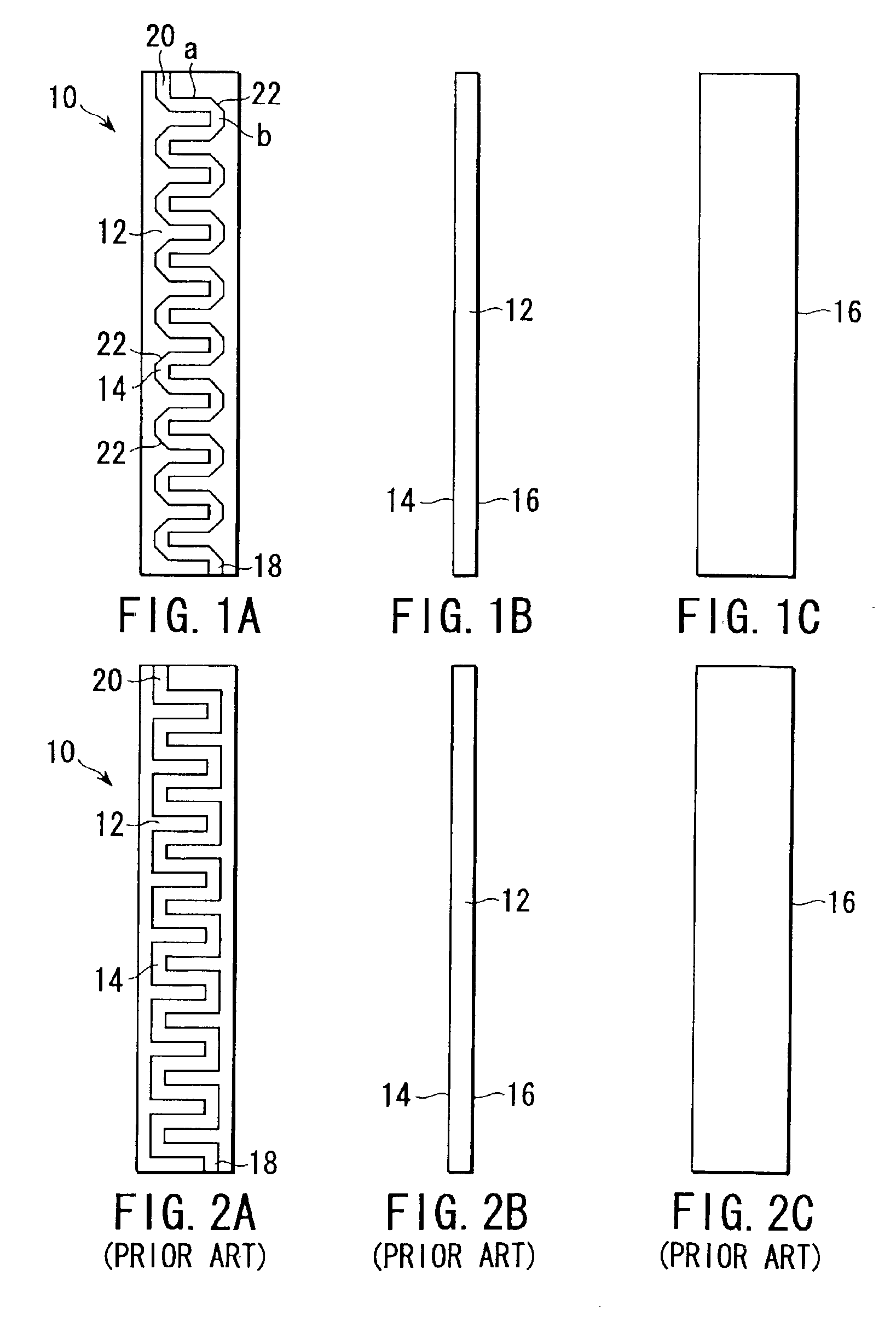
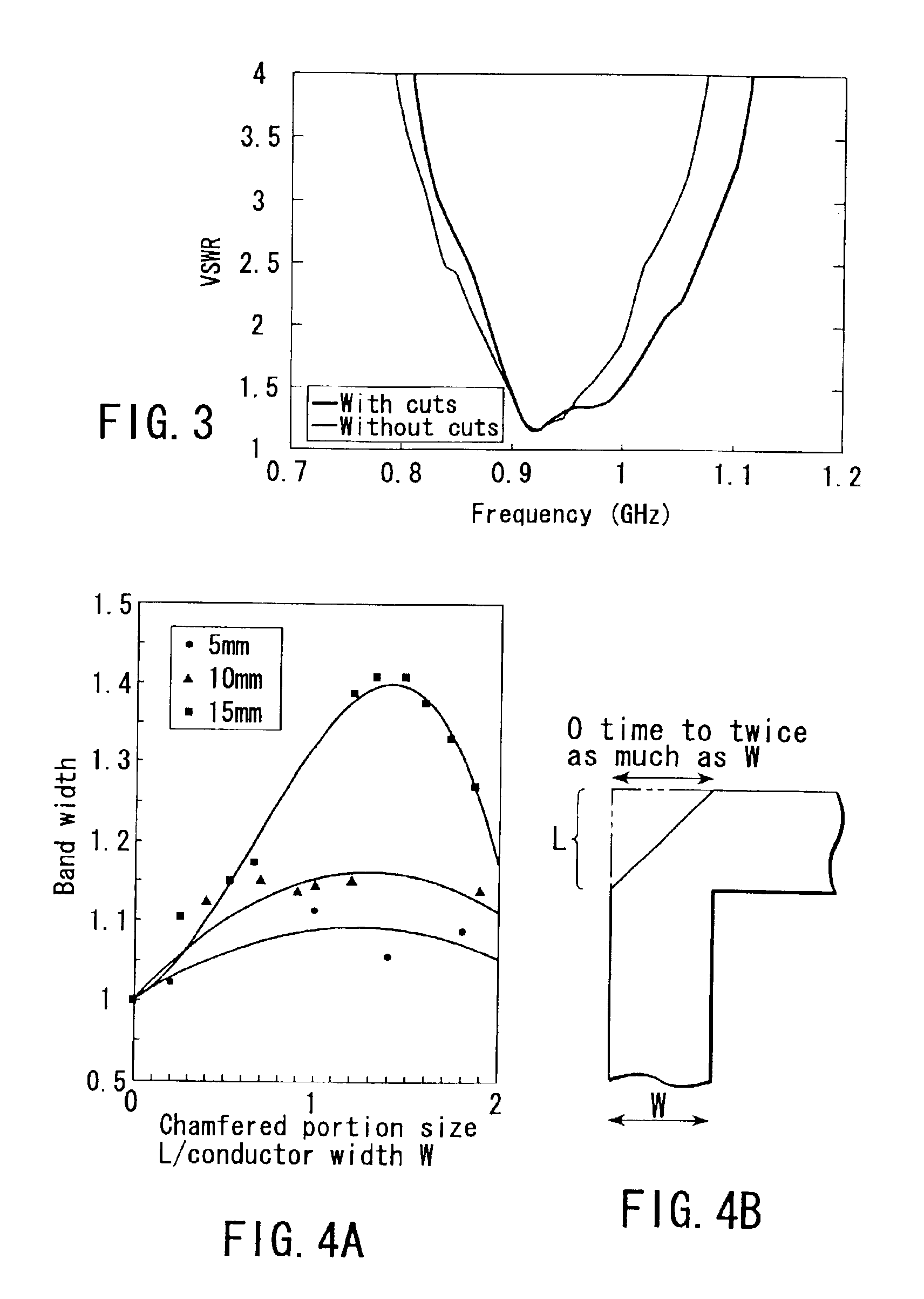
[0046]Comparison test results of a line-shaped antenna according to the first embodiment of the present invention and a conventional line-shaped antenna experimentally manufactured will be described. As the line-shaped antenna according to the first embodiment of the present invention, the line-shaped antenna 10 having the chamfered portions 22 as shown in FIGS. 1A to 1C are experimentally manufactured. For the experimentally manufactured line-shaped antenna 10, the dielectric substrate 12 has a length of 36 mm, width of 8 mm, and thickness of 1.6 mm. The antenna element 14 has a conductor width of 1 mm, conductor interval of 1 mm, and meander width of 6 mm. Moreover, the metal plate 16 has the same length and width as those of the dielectric substrate 12. For comparison with the above-described experimentally manufactured example, as the conventional line-shaped antenna, the line-shaped antenna 10 shown in FIGS. 2A to 2C is experimentally manufactured, and is the same as the line-s...
trial example 2
[0049]An example in which the size of the chamfered portion 22 is changed will be described.
[0050]As shown in FIG. 4B, three types of line-shaped antennas having conductor widths of 5 mm, 10 mm, and 15 mm are prepared. Moreover, the bandwidths are measured, when the size (length L of one of two equal sides of the portion chamfered in a right-angled isosceles triangle) of the chamfered portion is changed in a range of 0 to twice the conductor width W. Measurement results are shown in FIG. 4A. As shown in FIG. 4A, when the bandwidth without any chamfered portion is set to 1, and when the chamfered portions are provided, it is seen that the respective bandwidths change as follows.[0051](1) Conductor width 5 mm: bandwidth 1.00 to 1.09[0052](Maximum change amount ΔM=0.09)[0053](2) Conductor width 10 mm: bandwidth 1.00 to 1.16[0054](Maximum change amount ΔM=0.16)[0055](3) Conductor width 15 mm: bandwidth 1.00 to 1.40[0056](Maximum change amount ΔM=0.40)
[0057]In FIG. 4A, the change amount ...
PUM
| Property | Measurement | Unit |
|---|---|---|
| Size | aaaaa | aaaaa |
| Width | aaaaa | aaaaa |
| Deformation enthalpy | aaaaa | aaaaa |
Abstract
Description
Claims
Application Information
 - R&D
- Intellectual Property
- Life Sciences
- Materials
- Tech Scout
- Unparalleled Data Quality
- Higher Quality Content
- 60% Fewer Hallucinations
Browse by: Latest US Patents, China's latest patents, Technical Efficacy Thesaurus, Application Domain, Technology Topic, Popular Technical Reports.
© 2025 PatSnap. All rights reserved.Legal|Privacy policy|Modern Slavery Act Transparency Statement|Sitemap|About US| Contact US: help@patsnap.com


