
Photodiode array and method of making the same

a technology of photodiodes and arrays, applied in the field of photodiode arrays and a method of making the same, can solve the problems of limited filler, inability to form photodiodes, and practicability of forming through holes with a uniform diameter in a substrate having a thickness of 250 to 400 m

Active Publication Date: 2005-02-08
HAMAMATSU PHOTONICS KK
View PDF11 Cites 36 Cited by
  • Summary
  • Abstract
  • Description
  • Claims
  • Application Information

AI Technical Summary

Benefits of technology

Hence, it is an object of the present invention to overcome the problem mentioned above and provide a photodiode array which is less likely to cause conduction failures in through hole wirings, while yielding a large fill factor.
In this photodiode array, all the covering corners' angles of the conductive layer extending from the incident surface to the opposite surface by way of the wall surface of the through hole become 90° or greater, whereby conduction failures are less likely to occur because of insufficient coverage with the conductive layer. Also, even when the photodiodes are disposed close to each other, the fill factor can be increased.
This photodiode array comprises the high impurity concentration layer surrounding the through hole, and thus can trap unnecessary carriers which may occur when the through hole is mechanically damaged, thereby suppressing leak currents and dark currents.
In this method, the vertical hole is formed after the pyramidal depression having a quadrangular pyramid form is formed. Thus formed pyramidal depression has a depth smaller than the thickness of the semiconductor substrate. As a consequence, etching solutions do not leak to the second surface side, and thus do not adversely affect the photodiodes on the second surface side.

Problems solved by technology

Therefore, the photodiodes cannot be formed so close to each other, whereby the filler is limited.
Though dry etching may be used for forming a through hole perpendicular to the substrate surface, it is practically impossible to form a through hole with a uniform diameter in a substrate having a thickness of 250 to 400 μm.
Also, since the processing rate of dry etching is low, it takes a long processing time to penetrate through the substrate having a thickness of 250 to 400 μm.

Method used


Image

  • Photodiode array and method of making the same
  • Photodiode array and method of making the same
  • Photodiode array and method of making the same

Examples


Embodiment Construction

In the following, embodiments of the present invention will be explained. Here, constituents identical to each other will be referred to with numerals identical to each other without repeating overlapping descriptions.

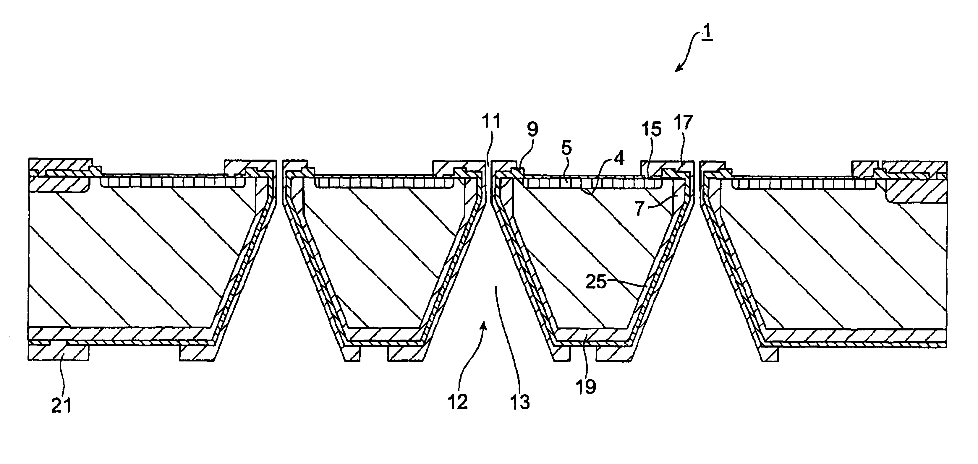
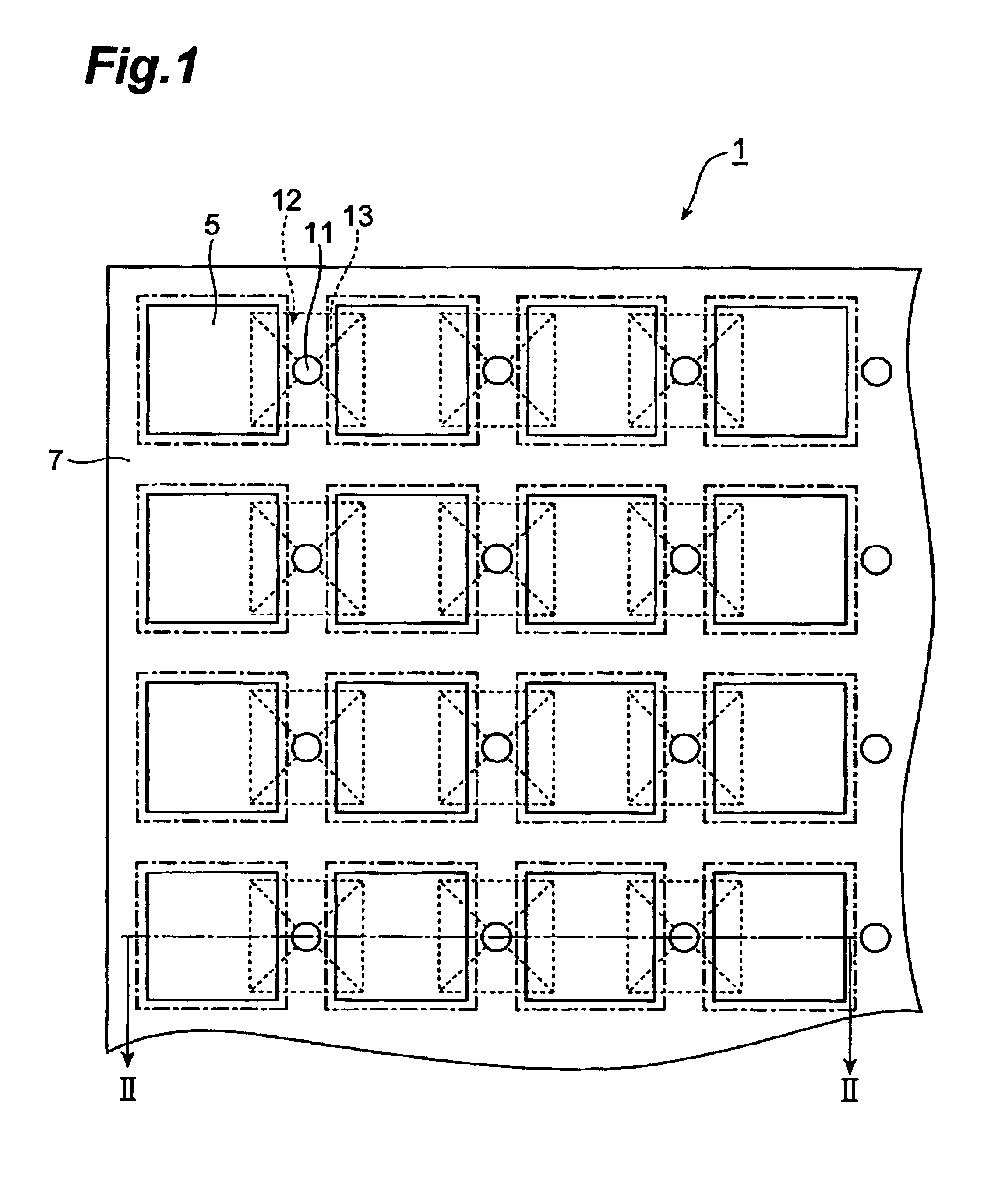
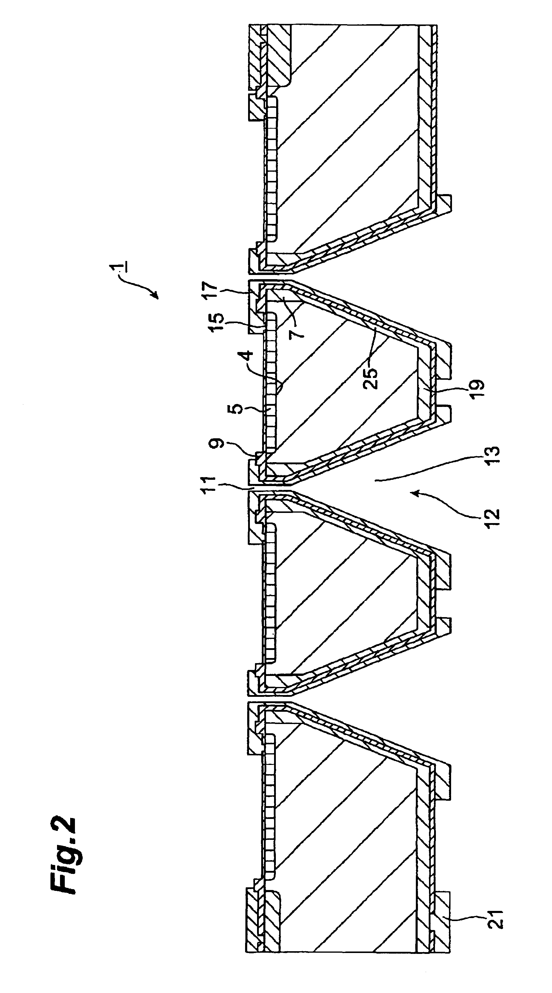
FIG. 1 is a plan view enlarging a part of the photodiode array in accordance with a first embodiment, whereas FIG. 2 is a sectional view thereof.

In the following explanation, the surface on which light is incident will be referred to as front side, whereas the surface opposite therefrom will be referred to as rear side. In the photodiode array 1 of this embodiment, a plurality of pn junctions (photodiodes) 4 are regularly arranged in an array of a matrix on the front side, each pn junction functioning as a photo-sensitive pixel of the photodiode array 1.

The photodiode array 1 comprises an n-type silicon substrate 3 having a thickness of 270 μm and an impurity concentration of 1×10¹² to 1015 / cm3; and a plurality of p-type impurity diffusion layers 5 arranged with a pitc...


PUM


Abstract

A photodiode array comprises a semiconductor substrate formed with an array of a plurality of pn junction type photodiodes on a light incident surface side, the surface opposite from the incident surface in the semiconductor substrate being made of a (100) plane; a through hole, formed in an area held between the photodiodes, penetrating through the semiconductor substrate from the incident surface side to the opposite surface side; and a conductive layer extending from the incident surface to the opposite surface by way of a wall surface of the through hole; the through hole being formed by connecting a vertical hole part formed substantially perpendicular to the incident surface on the incident surface side, and a pyramidal hole part formed like a quadrangular pyramid on the opposite surface side to each other within the semiconductor substrate; the pyramidal hole part having a wall surface formed as a (111) plane.

Description

BACKGROUND OF THE INVENTION1. Field of the InventionThe present invention relates to a photodiode array and a method of making the same.2. Related Background ArtPhotodiode arrays for CT (computed tomography) have been required to have a larger area. For eliminating insensible regions from a photodiode array, three-dimensional packaging is necessary, in which a signal processing unit is disposed on the opposite side (rear side) of the light incident surface. To this aim, it is necessary for an electrode formed on the incident side (front side) by using a through hole wiring to be drawn to the opposite side (rear side) of the incident surface.Semiconductor devices using such a through hole wiring are disclosed, for example, in the following Patent Documents 1 and 2. In the semiconductor device disclosed in the Patent Document 1, a substrate is etched by wet etching with an alkali solution in order to form a through hole, whereby the revealed plane of substrate is at an angle of 54.7° ...

Claims


Application Information

Patent Timeline
IPC IPC(8): G01J1/10G01J1/24H01L31/00H01L27/146
CPCH01L27/14643H01L27/14634H01L27/14687H01L27/14636H01L21/76898
Inventor SHIBAYAMA, KATSUMI
Owner HAMAMATSU PHOTONICS KK
Learn More