
Semiconductor package and method for manufacturing the same

a technology of semiconductors and packages, applied in the direction of semiconductor devices, semiconductor/solid-state device details, electrical apparatus, etc., can solve the problems of reducing or diminishing the utility of certain applications of packages having superior heat dissipation capabilities, and achieve the effect of light, thin, and simple structur

Inactive Publication Date: 2005-01-25
AMKOR TECH SINGAPORE HLDG PTE LTD
View PDF350 Cites 37 Cited by
  • Summary
  • Abstract
  • Description
  • Claims
  • Application Information

AI Technical Summary

Benefits of technology

The present invention provides various embodiments of a heat dissipating semiconductor package and related methods for manufacturing the same. The semiconductor package includes a semiconductor die which is mechanically and electrically connected to a plurality of leads through the use of conductive bumps. The orientation of the leads relative to the semiconductor die, coupled with the use of the conductive bumps, facilitates a significant reduction in the overall thickness of the semiconductor package, resulting in a light, thin, and simple structure. Additionally, prescribed regions or surfaces of the leads are exposed within the encapsulating portion of the semiconductor package, which maximizes the heat discharging efficiency of the semiconductor package. The present invention provides a solution for improving heat dissipation in semiconductor packages and ensuring their reliability and durability.

Problems solved by technology

However, semiconductor packages having superior heat dissipation capabilities are often of a size which decreases or diminishes their utility in certain applications.

Method used


Image

  • Semiconductor package and method for manufacturing the same
  • Semiconductor package and method for manufacturing the same
  • Semiconductor package and method for manufacturing the same

Examples


first embodiment

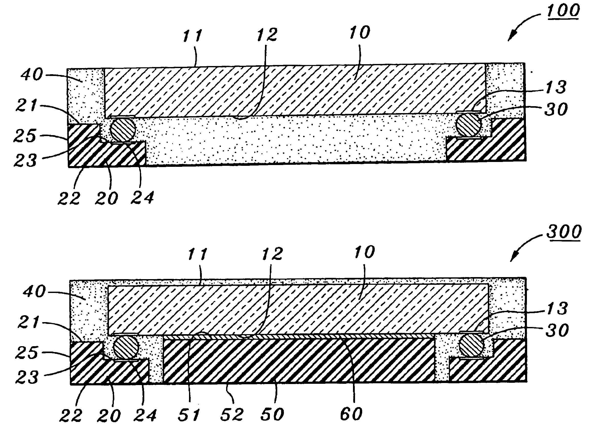
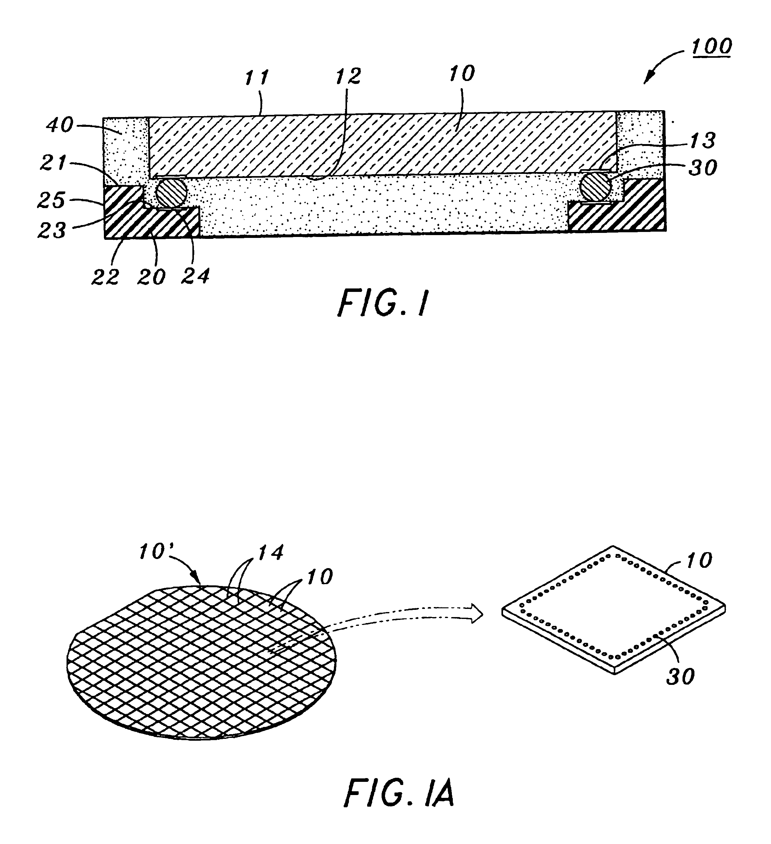
Referring now to the drawings wherein the showings are for purposes of illustrating preferred embodiments of the present invention only, and not for purposes of limiting the same, FIG. 1 illustrates in cross section a semiconductor package 100 constructed in accordance with the present invention. The semiconductor package 100 includes a semiconductor die 10 which defines a generally planar first surface 11 and a generally planar second surface 12 which is disposed in opposed relation to the first surface 11. Located on the second surface 12 of the semiconductor die 10 adjacent the peripheral edge thereof are a plurality of bond pads 13 which are used for routing electrical signals to and from the semiconductor die 10.

In addition to the semiconductor die 10, the semiconductor package 100 includes a plurality of leads 20 which are disposed about the periphery of the second surface 12 of the semiconductor die 10 in spaced relation thereto. Each of the leads 20 defines a generally plana...

third embodiment

In the semiconductor package 300 of the third embodiment, the first surface 11 of the semiconductor die 10 is encapsulated by the encapsulant (i.e., covered by the encapsulating portion 40). As a result, the first surface 11 of the semiconductor die 10 is not exposed within the encapsulating portion 40 to the outside of the semiconductor package 300. Since the semiconductor die 10 is located on the inside of the encapsulating portion 40, the bonding force between the encapsulating portion 40 and the semiconductor die 10 is increased, with the semiconductor die 10 being more positively protected from the external environment. Since the second surface 52 of the die paddle 50 is exposed within the bottom surface of the encapsulating portion 40, the heat generated by the semiconductor die 10 is still rapidly emitted to the outside of the semiconductor package 300.

Referring now to FIGS. 3A-3D regarding a preferred manufacturing method for the semiconductor package 300 of the third embodi...


PUM


Abstract

A semiconductor package is provided which includes a semiconductor die having opposed, generally planar first and second surfaces and a peripheral edge. Formed on the second surface of the semiconductor die in close proximity to the peripheral edge thereof is a plurality of bond pads. The semiconductor package further includes a plurality of leads which are positioned about the peripheral edge of the semiconductor die in space relation to the second surface thereof. Each of the leads includes opposed, generally planar first and second surfaces, and a generally planar third surface which is oriented between the first and second surfaces in opposed relation to a portion of the second surface. In the semiconductor package, a plurality of conductive bumps are used to electrically and mechanically connect the bond pads of the semiconductor die to the third surfaces of the respective ones of the leads. An encapsulating portion is applied to and partially encapsulates the leads, the semiconductor die, and the conductive bumps.

Description

STATEMENT RE: FEDERALLY SPONSORED RESEARCH / DEVELOPMENT(Not Applicable)BACKGROUND OF THE INVENTION1. Field of the InventionThe present invention relates generally to semiconductor packages, and more particularly to a semiconductor package which is specifically configured to maximize the dissipation or discharge of heat generated from the semiconductor die thereof.2. Description of the Related ArtA recent trend in the electronics industry has been to develop semiconductor package structures which maximize the dissipation or discharging effect of heat generated from the semiconductor die of the package. However, semiconductor packages having superior heat dissipation capabilities are often of a size which decreases or diminishes their utility in certain applications. The present invention is specifically adapted to address this deficiency by providing a semiconductor package having superior heat dissipation capabilities and simple, light, thin and miniature structural characteristics, ...

Claims


Application Information

Patent Timeline
Patent Type & Authority Patents(United States)
IPC IPC(8): H01L23/28H01L23/31H01L23/04
CPCH01L23/3114H01L2224/16245H01L2924/18161H01L2924/01078H01L2924/01079H01L2224/32245H01L2224/45144H01L2224/05571H01L2224/05573H01L2924/00014H01L2924/00H01L2224/05599H01L23/04
Inventor PAEK, JONG SIK
Owner AMKOR TECH SINGAPORE HLDG PTE LTD
Learn More