
Bad pixel detection and correction in an image sensing device

a technology of image sensing and bad pixel, which is applied in the field of image sensing devices, can solve the problems of unfavorable image generation, unfavorable image generation, and possible economic unfeasibility and unrealizability, and achieve the effects of brighter than expected spots in the generated image, stringent and perhaps economic unfeasibility, and unrealizability

Inactive Publication Date: 2004-05-18
OVONYX MEMORY TECH LLC
View PDF16 Cites 86 Cited by
  • Summary
  • Abstract
  • Description
  • Claims
  • Application Information

AI Technical Summary

Benefits of technology

The present invention relates to an image sensing device comprising an array of photodetectors and the detection and correction of bad pixels in such a device. The technical effect of the invention is to provide a method for detecting and correcting bad pixels in an image sensing device, which can improve the quality of the generated image.

Problems solved by technology

Even with a semiconductor manufacturing process having a 99% yield, it is recognized that the sensing device array will inevitably include a number of bad photodetectors (also referred to herein as "bad pixels").
Requiring a semiconductor production line to produce sensors without any bad pixels is a very stringent and perhaps an economically unfeasible and unrealizable demand.
A bad pixel within a sensor may arise in a number of ways.
This defect produces a brighter than expected spot in the generated image.
Second, the signal output from the photodetector may always give a low reading (a "dead pixel").
This defect produces a darker that expected spot in the generated image.
Third, a signal proportional to the incident light may be generated, but (due, for example, to incorrect photodiode gain, dark current and / or offset) does not accurately represent of the incident light in the sense that it differs from signals generated by other similarly situated photodetectors (a "noisy pixel").
This defect produces an erroneous spot (color, intensity, contrast, and the like) in the generated image.
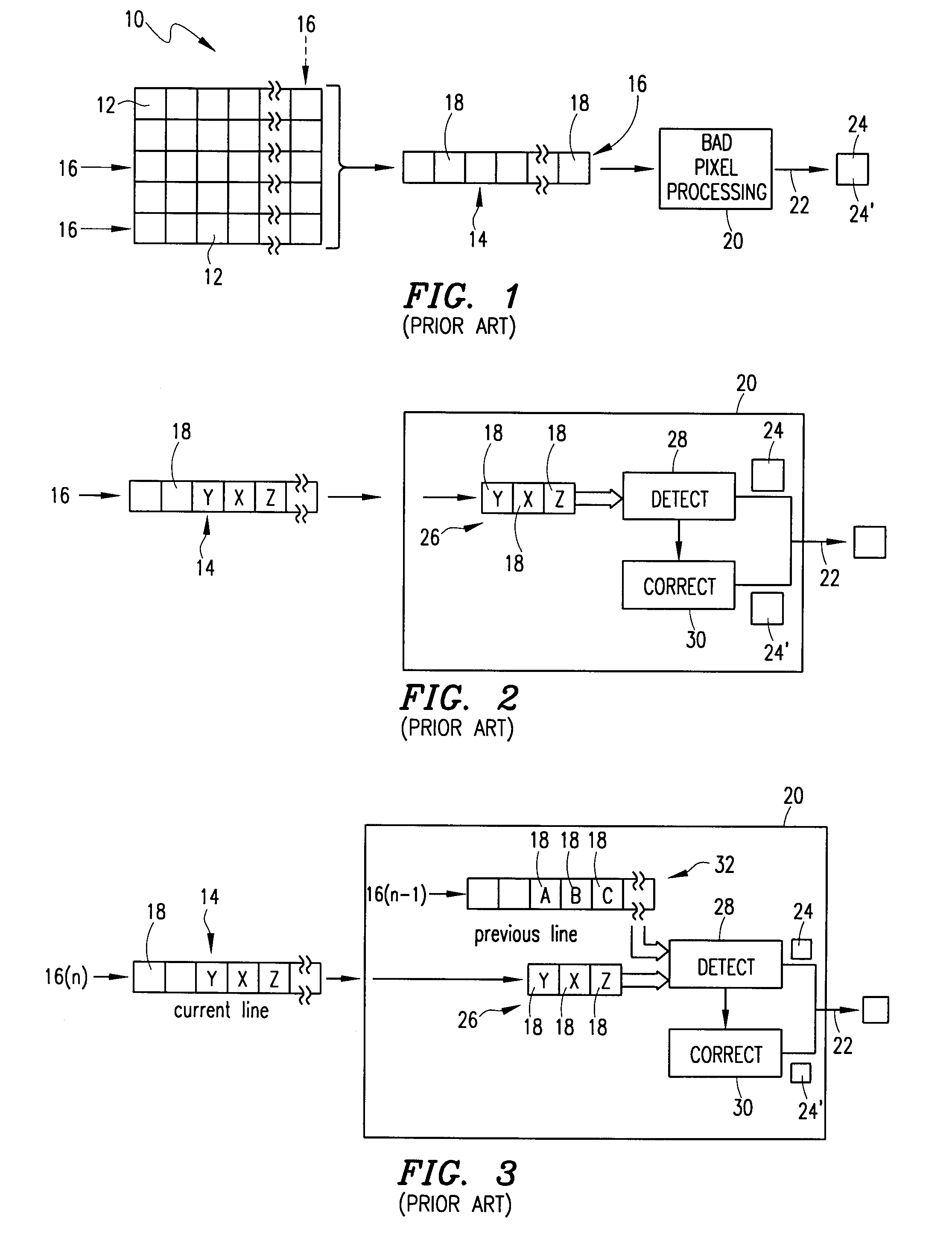
However, the operation illustrated in FIG. 3 has a significant memory overhead requirement.

Method used


Image

  • Bad pixel detection and correction in an image sensing device
  • Bad pixel detection and correction in an image sensing device
  • Bad pixel detection and correction in an image sensing device

Examples


Embodiment Construction

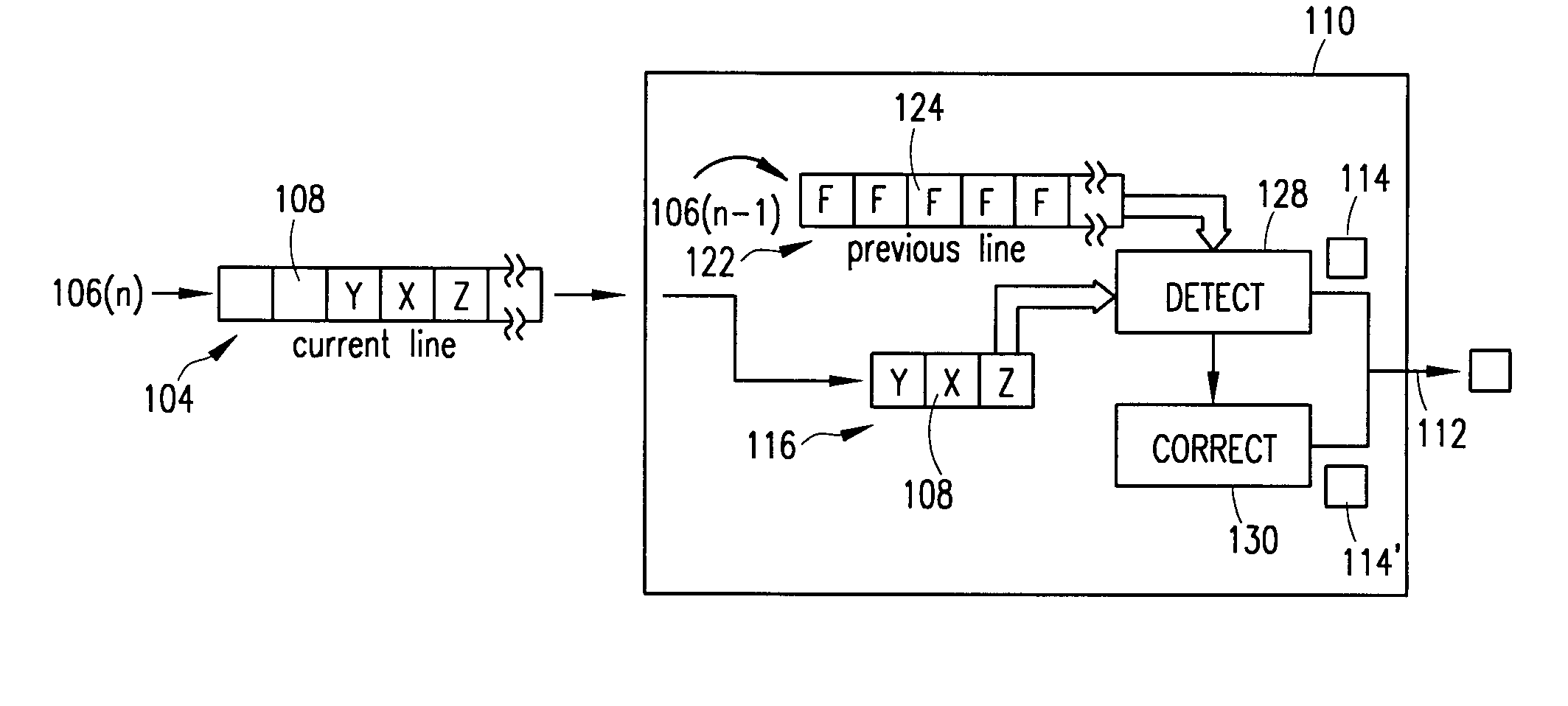
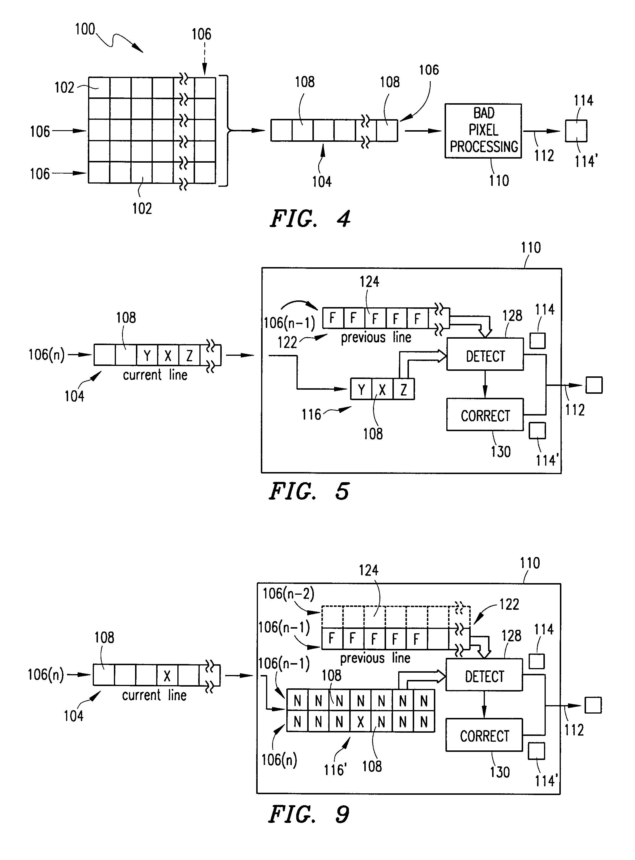
FIG. 4 shows a simplified schematic diagram of a sensor read-out operation in accordance with an embodiment of the present invention. A sensor array 100 includes a plurality of photodetectors 102. Each photodetector 102 outputs a signal (referred to herein as "pixel data") whose magnitude ideally has a predetermined monotonic relationship to the intensity of light incident on the photodetector. Although not explicitly shown, the generated signal for each pixel has a digital format (obtained through appropriate analog-to-digital conversion) normally ten to twelve bits in size.

A read-out buffer 104 is used to read out and capture either a horizontal row or vertical column of individual pixel data that is generated from the photodetectors. In this context, a horizontal row or a vertical column is referred to as a "line" 106. Following capture of a line 106 of pixel data in the buffer 104, each individual piece of pixel data 108 is serially processed in a bad pixel processor 110. The pr...


PUM


Abstract

A sensor includes an array of photodetectors each generating an output signal of pixel data indicative of incident light intensity. This pixel data is read out from the array one line at a time and stored in a line buffer. A bad pixel processor includes a first buffer that stores pixel data obtained from the line buffer for a certain pixel in a currently read out line and pixel signal light data for pixels adjacent to the certain pixel.

Description

1. Technical Field of the InventionThe present invention relates to an image sensing device comprising an arrayed plurality of photodetectors and, in particular, to the detection of bad pixels in such a device and the correction of pixel data output from those bad pixels.2. Description of Related ArtIt is well known in the art to assemble a plurality of photodetectors (also referred to in the art as "photosites") in an array format to create an image sensing device. Each individual photodetector operates to output a signal whose magnitude is proportional to the intensity of light incident on the site of the photodetector. These output signals can then be subsequently processed and manipulated to generate an image comprised of a plurality of individual picture elements (also referred to in the art as "pixels"), wherein each pixel in the image corresponds with one of the photodetectors.The individual photodetectors used in such a sensing device are typically photodiodes that are forme...

Claims


Application Information

Patent Timeline
Patent Type & Authority Patents(United States)
IPC IPC(8): H04N5/217H01L27/14G06T1/00H04N1/028H04N5/367
CPCH04N5/367H04N25/68
Inventor BAHARAV, IZHAKKAKARALA, RAMAKRISHNAZHANG, XUEMEIVOOK, DIETRICH WERNER
Owner OVONYX MEMORY TECH LLC
Learn More