Graphene nanostructure
Active Publication Date: 2021-03-04
TOYOTA CENT RES & DEV LAB INC
View PDF1 Cites 0 Cited by
- Summary
- Abstract
- Description
- Claims
- Application Information
AI Technical Summary
Benefits of technology
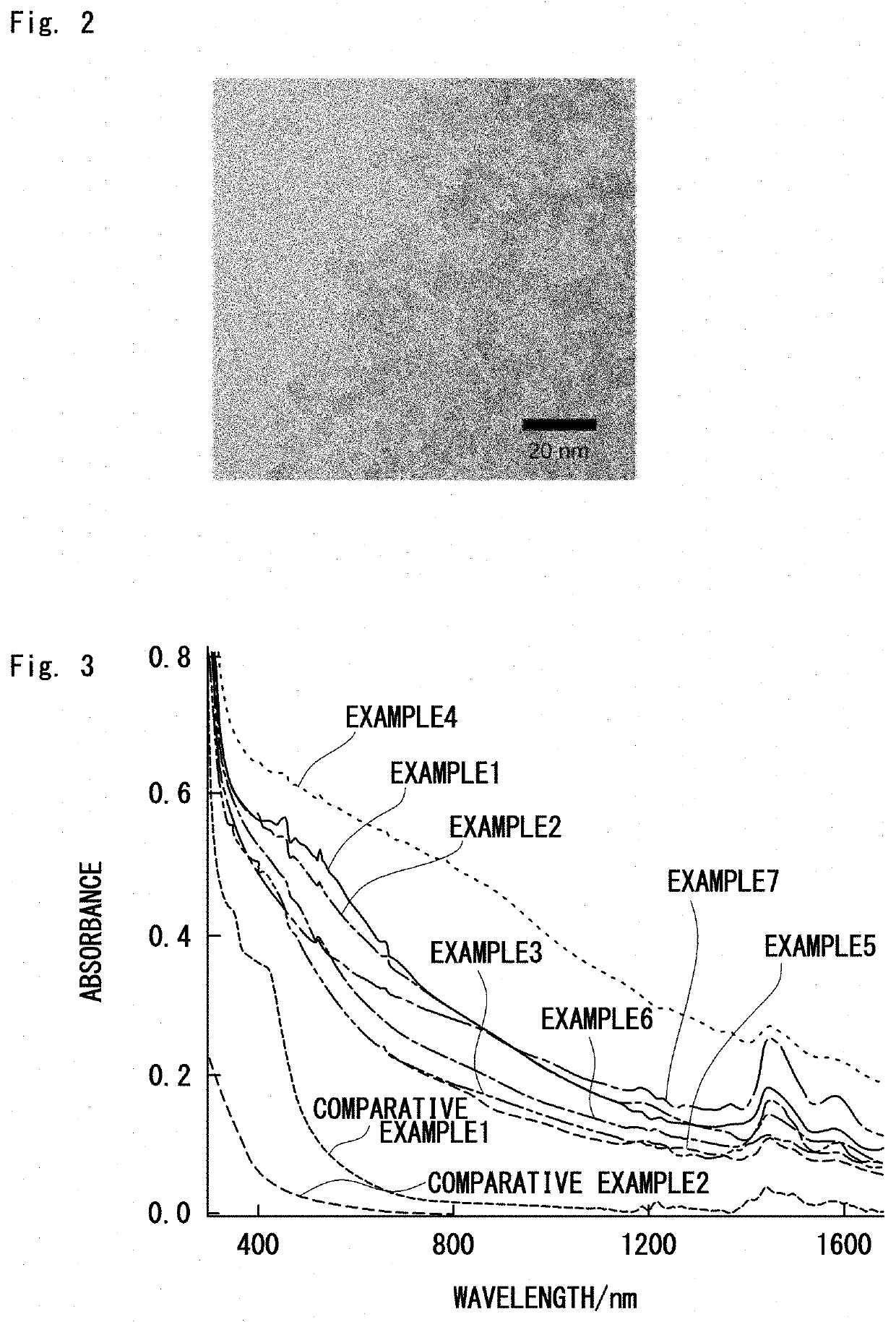
[0091]A nanographene has semiconductivity (band gap Eg>0 eV) and can absorb light. The nanographene, however, has low light sensitivity over the entire wavelength range and particularly has almost no sensitivity in an infrared region with a wavelength of 1,000 nm or more. On the other hand, when the size of a nanographene is increased, a light absorption edge can be shifted to a longer wavelength to some extent (about 600 to 700 nm). Only by optimizing the size of a nanographene, however, a light absorption edge cannot be shifted to 1,000 nm or more.
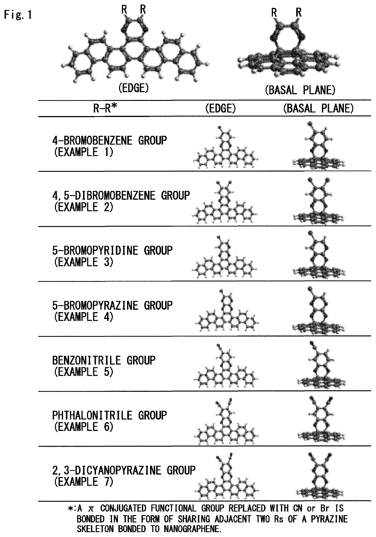
[0092]On the contrary, when a π conjugated functional group is introduced into a nanographene via a pyrazine skeleton, light sensitivity in a short wavelength range improves. In addition to that, when a Br group and/or a CN group are/is introduced into the π conjugated functional group, the light sensitivity in a short wavelength range improves further as well as a light absorption edge is shifted to a longer wavelength of 1,000 nm or more, and the light sensitivity in a long wavelength range improves significantly.
[0093]A nanographene has an electron-donating proper
Problems solved by technology
A problem, however, is that a graphene has metallic properties and the sensitivity of an optical sensor using the graphene is low.
Only by optimizing the size of a graphene nanostructure, how
Method used
View moreImage
Smart ImageViewing Examples
Examples
 PUM
 Abstract
A graphene nanostructure has a nanographene, a π conjugated functional group bonded to the nanographene via a pyrazine skeleton, and at least one Br group and/or at least one CN group introduced into the π conjugated functional group. A graphene nanostructure preferably has an average size of 1 nm or larger to 100 nm or smaller, a band gap of 0.01 eV or higher to 1.2 eV or lower, and/or a HOMO level of −6.0 eV or higher to −4.0 eV or lower. As the π conjugated functional group into which the Br group(s) and/or the CN group(s) are/is introduced, a 4-bromobenzene group, a 4,5-dibromobenzene group, a 5-bromopyridine group, a 5-bromopyrazine group, a benzonitrile group, a phthalonitrile group, or a 2,3-dicyanopyrazine group is desirable.
Description
FIELD OF THE INVENTION[0001]The present invention relates to a graphene nanostructure, more specifically, a graphene nanostructure that can detect light from deep ultraviolet to infrared with a wavelength of 1,000 nm or more and can be used as a broadband optical sensor.BACKGROUND OF THE INVENTION[0002]A graphene is a sheet material comprising one atomic layer to several atomic layers of a graphite crystal, and has the characteristics of an extremely high carrier mobility at room temperature and being able to absorb light of all wavelengths from deep ultraviolet to terahertz. An attempt therefore is being made to create a broadband optical sensor responsive to light from deep ultraviolet to infrared by using such unique properties of a graphene. A problem, however, is that a graphene has metallic properties and the sensitivity of an optical sensor using the graphene is low.[0003]Meanwhile, when a graphene is refined to a size of several nanometers, a graphene nanostructure converted...
Claims
Login to View More Application Information
Patent Timeline
 IPC IPC(8): C07D241/12C01B32/194C07D403/04C07D401/04H01L51/00H01L51/42
CPCC07D241/12C01B32/194C07D403/04B82Y15/00H01L51/0045H01L51/428C07D401/04H01L31/10B82Y30/00B82Y40/00C01B2204/22C01B2204/32H10K30/65H10K85/20
Inventor TETSUKA, HIROYUKI
Owner TOYOTA CENT RES & DEV LAB INC
Features
- R&D
- Intellectual Property
- Life Sciences
- Materials
- Tech Scout
- Unparalleled Data Quality
- Higher Quality Content
- 60% Fewer Hallucinations
Learn More Browse by: Latest US Patents, China's latest patents, Technical Efficacy Thesaurus, Application Domain, Technology Topic, Popular Technical Reports.
© 2025 PatSnap. All rights reserved.Legal|Privacy policy|Modern Slavery Act Transparency Statement|Sitemap|About US| Contact US: help@patsnap.com


