Light-emitting device, and electronic apparatus
- Summary
- Abstract
- Description
- Claims
- Application Information
AI Technical Summary
Benefits of technology
Problems solved by technology
Method used
Image
Examples
first embodiment
1. First Embodiment
Overview of Light-Emitting Device
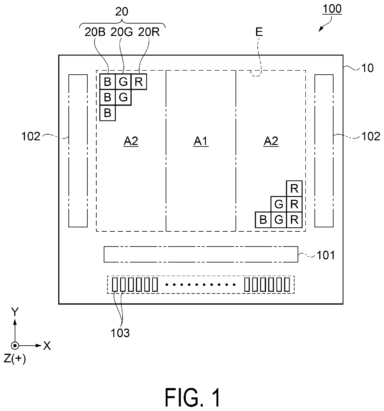
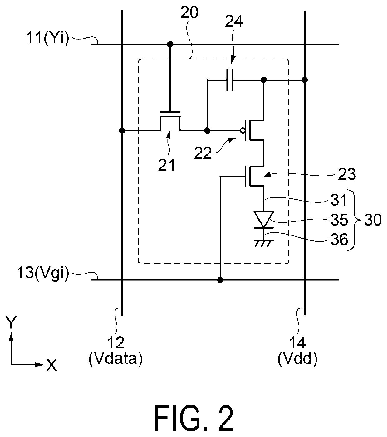
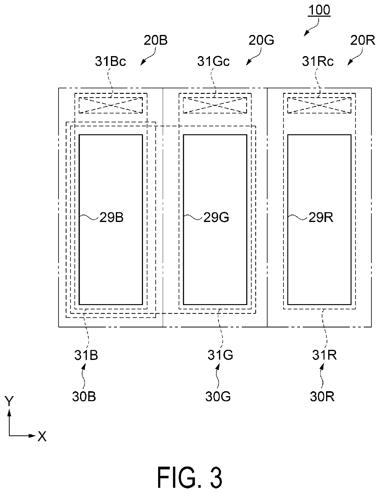
[0041]First, an organic EL device as an example of a light-emitting device according to this embodiment will be described with reference to FIGS. 1 to 3. FIG. 1 is a schematic plan view illustrating a configuration of the organic EL device. FIG. 2 is an equivalent circuit diagram illustrating an electrical configuration of a light-emitting pixel in the organic EL device. FIG. 3 is a schematic plan view illustrating a configuration of a light-emitting pixel in the organic EL device.
[0042]As illustrated in FIG. 1, an organic EL device 100 as an example of a light-emitting device includes an element substrate 10, a plurality of light-emitting pixels 20 arranged in a matrix in a display region E of the element substrate 10, a data line drive circuit101 and a scanning line drive circuit 102 as peripheral circuits that drive and control the plurality of light-emitting pixels 20, and a plurality of external connection terminals 103 used t...
second embodiment
2. Second Embodiment
Division of Display Area
[0184]FIGS. 13A to 13D are diagrams illustrating divided display areas.
[0185]The first embodiment deals with an exemplary case where the display region is divided into two areas, but the present disclosure is not limited to this configuration and the display region may be divided into a plurality of areas. The same components as in the first embodiment are given the same reference signs, and redundant descriptions of these components will be omitted. Note that in the following description, the X direction is horizontal, the Y direction is vertical, the +X direction is right, the −X direction is left, the +Y direction is up and the −Y direction is down.
[0186]In FIG. 13A, the display region E of the organic EL device 100 is divided into n areas each having a vertical stripe shape. Specifically, with a center area of the display region E in the X direction defined as an area A1, the display region E is divided until an area An in the order of...
third embodiment
3. Third Embodiment
Method for Manufacturing Second Adjustment Layer
[0201]FIG. 14 is a process flow chart illustrating a flow of manufacturing the adjustment layer. FIGS. 15A to 15C are cross-sectional views illustrating manufacturing processes in individual steps.
[0202]Here, a method for manufacturing an adjustment layer that is different to the manufacturing method of the first embodiment will be described with reference to FIG. 14 and FIGS. 15A to 15C. The same components as in the first embodiment are given the same reference signs, and redundant descriptions of these components will be omitted.
[0203]First, in process diagram 131 in FIG. 15A, layers until the second protective layer 26 that serves as the foundation of the adjustment layer are formed on the base material 10s. The second protective layer 26 is a flat silicon nitride layer formed on the first protective layer 18.
[0204]In Step S11, a material layer 52 is formed. The material layer 52 is formed to fill spaces on the e...
PUM
 Abstract
Description
Claims
Application Information
 - R&D
- Intellectual Property
- Life Sciences
- Materials
- Tech Scout
- Unparalleled Data Quality
- Higher Quality Content
- 60% Fewer Hallucinations
Browse by: Latest US Patents, China's latest patents, Technical Efficacy Thesaurus, Application Domain, Technology Topic, Popular Technical Reports.
© 2025 PatSnap. All rights reserved.Legal|Privacy policy|Modern Slavery Act Transparency Statement|Sitemap|About US| Contact US: help@patsnap.com


