
Optical and electrical secondary path rejection

a secondary path and optical technology, applied in the field of integrated devices, can solve the problem that the ability of massive parallel analysis of biological or chemical samples is typically limited to laboratory settings

Pending Publication Date: 2020-12-31
QUANTUM SI
View PDF33 Cites 4 Cited by
  • Summary
  • Abstract
  • Description
  • Claims
  • Application Information

AI Technical Summary

Benefits of technology

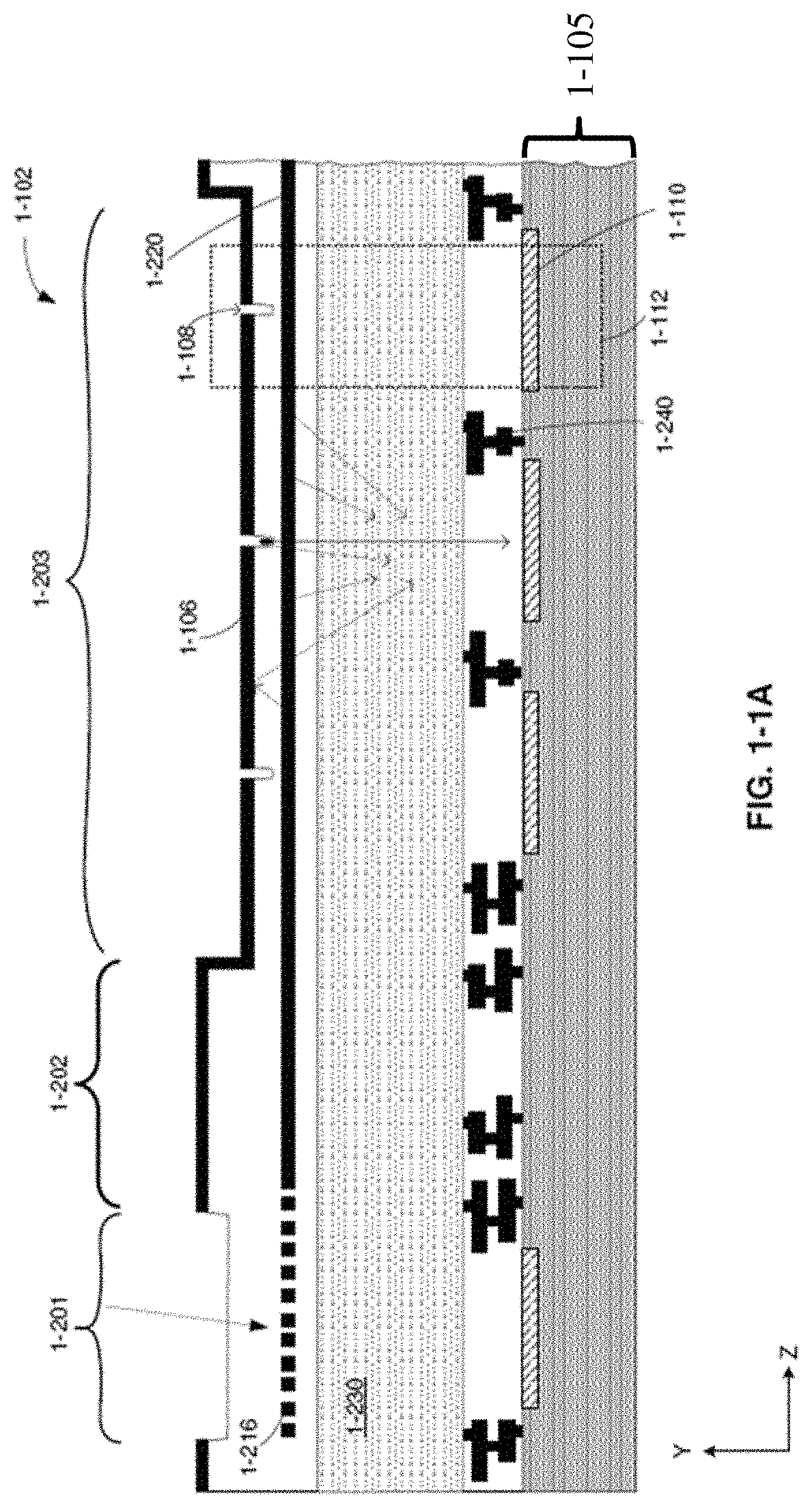
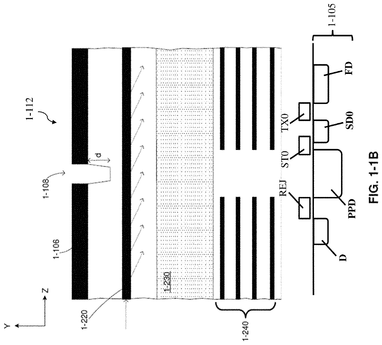
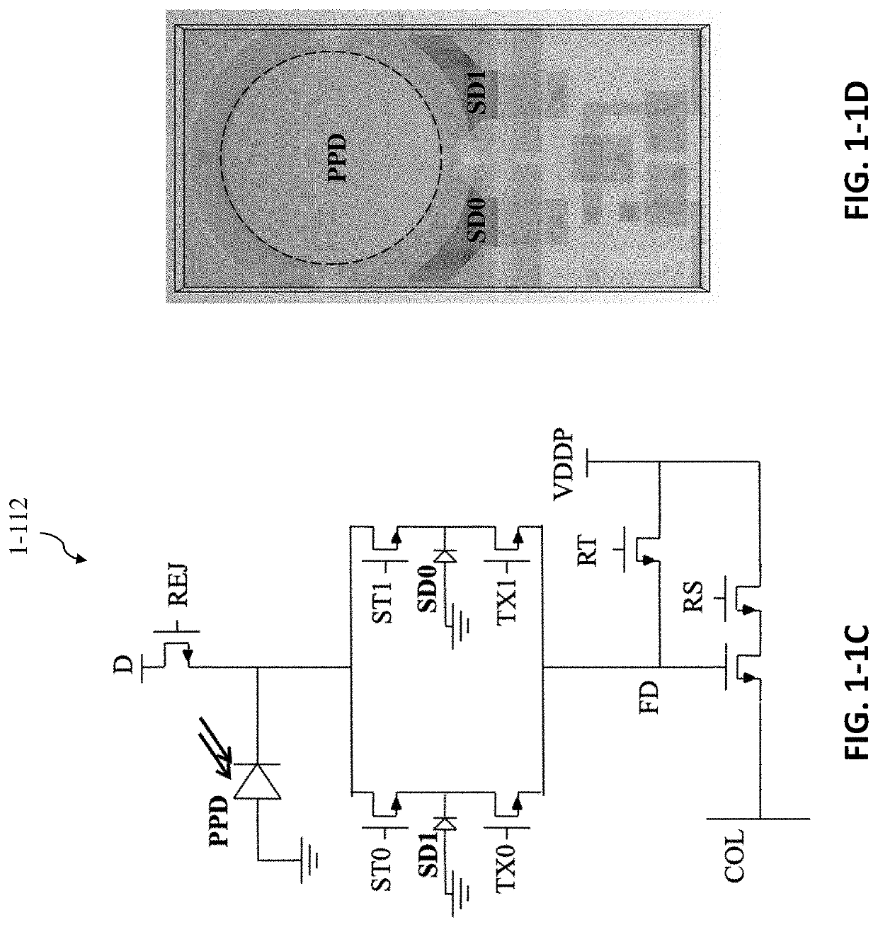
The present disclosure relates to an integrated device that includes a photodetection region, one or more storage bins, and an optical barrier to block at least some photons and charge carriers from reaching the storage bins. The optical barrier may be an at least partially opaque component, such as a contact or a metal layer, positioned along the path of the emitted photons. The device may also include a transfer gate to control the flow of charge carriers from the photodetection region to the storage bins. The technical effects of this invention include improved signal-to-noise ratios, improved image quality, and improved control of charge carrier flow.

Problems solved by technology

Instruments that are capable of massively-parallel analyses of biological or chemical samples are typically limited to laboratory settings because of several factors that can include their large size, lack of portability, requirement of a skilled technician to operate the instrument, power need, need for a controlled operating environment, and cost.

Method used


Image

  • Optical and electrical secondary path rejection
  • Optical and electrical secondary path rejection
  • Optical and electrical secondary path rejection

Examples


Embodiment Construction

I. Introduction

[0123]Aspects of the present disclosure relate to integrated devices, instruments and related systems capable of analyzing samples in parallel, including identification of single molecules and nucleic acid sequencing. Such an instrument may be compact, easy to carry, and easy to operate, allowing a physician or other provider to readily use the instrument and transport the instrument to a desired location where care may be needed. Analysis of a sample may include labeling the sample with one or more fluorescent markers, which may be used to detect the sample and / or identify single molecules of the sample (e.g., individual nucleotide identification as part of nucleic acid sequencing). A fluorescent marker may become excited in response to illuminating the fluorescent marker with excitation light (e.g., light having a characteristic wavelength that may excite the fluorescent marker to an excited state) and, if the fluorescent marker becomes excited, emit emission light ...


PUM


Abstract

Described herein are techniques to reduce or remove the impact of secondary path photons and / or charge carriers on storage bins of an integrated device to improve noise performance, and thus, sample analysis. Some embodiments relate to optical rejection techniques such as including an optical barrier positioned to block at least some photons from reaching the storage bins. Some embodiments relate to electrical rejection techniques such as including an electrical barrier configured to block at least some charge carriers from reaching the storage bins along at least one secondary path. Some embodiments relate to an integrated device in which at least one storage bin is shaped and / or positioned relative to the photodetector to facilitate receipt of some charge carriers (e.g., fluorescent emission charge carriers) and / or photons and to impede receipt of other charge carriers (e.g., noise charge carriers) and / or photons.

Description

RELATED APPLICATIONS[0001]This application claims priority under 35 U.S.C. § 119(e) to U.S. Provisional Application Ser. No. 62 / 868,829, filed Jun. 28, 2019 under Attorney Docket No.: R0708.70074US00, and entitled, “OPTICAL AND ELECTRICAL SECONDARY PATH REJECTION,” which is herein incorporated by reference in its entirety.FIELD OF THE DISCLOSURE[0002]The present disclosure relates to integrated devices and related instruments that can perform massively-parallel analyses of samples by providing short optical pulses to tens of thousands of sample wells or more simultaneously and receiving fluorescent signals from the sample wells for sample analyses. The instruments may be useful for point-of-care genetic sequencing and for personalized medicine.BACKGROUND[0003]Instruments that are capable of massively-parallel analyses of biological or chemical samples are typically limited to laboratory settings because of several factors that can include their large size, lack of portability, requi...

Claims


Application Information

Patent Timeline
IPC IPC(8): G01N21/64
CPCG01N2021/6439G01N2021/6463G01N21/6428H01L27/14623G01N21/6454G01N21/648G01N21/7703G01N2201/064G01N2021/6441H01L27/14621H01L27/14625H01L27/14609H01L27/14636H04N25/771
Inventor YANG, DAJIANGGHASEMI, FARSHIDFIFE, KEITH G.REARICK, TODDKABIRI, ALISCHMID, GERARDWEBSTER, ERIC A.G.
Owner QUANTUM SI
Learn More