Imaging lens assembly and electronic device

a technology of plastic lens elements and electronic devices, applied in the field of compact imaging lens components, can solve the problems of difficult application of compact and high-precision plastic lens elements, inability to effectively attenuate stray light reflected from the surface of plastic lens elements,

Active Publication Date: 2020-01-02
LARGAN PRECISION
View PDF0 Cites 2 Cited by
  • Summary
  • Abstract
  • Description
  • Claims
  • Application Information

AI Technical Summary

Benefits of technology

The present disclosure describes an imaging lens assembly and an electronic device that includes the lens assembly and an image sensor. The lens assembly includes a plurality of lens elements, at least one of which is a dual molded lens element. The dual molded lens element has a light transmitting portion and a light absorbing portion. The light transmitting portion has an effective optical section and a first annular surface that connects the object-side surface and the image-side surface of the lens element. The light absorbing portion is located on at least one surface of the lens element and includes an opening and a second annular surface that also connects the first annular surface and the lens element's lens annular surface. The conditions for the effective optical section and the maximum outer diameter of the light transmitting portion and the light absorbing portion are described. The imaging lens assembly has improved image quality and color accuracy, and the electronic device has improved image quality and color accuracy.

Problems solved by technology

Accordingly, when the stray light is reflected from the surfaces of other optical elements of the imaging lens assembly to the surface of the plastic lens element, the stray light reflected from the surface of the plastic lens element cannot be effectively attenuated and would be incident on the surfaces of lens elements of the imaging lens assembly.
However, there are many limitations in implementation, so that they are difficult to be applied in compact and high-precision plastic lens elements.

Method used


Image

  • Imaging lens assembly and electronic device
  • Imaging lens assembly and electronic device
  • Imaging lens assembly and electronic device

Examples


1st embodiment

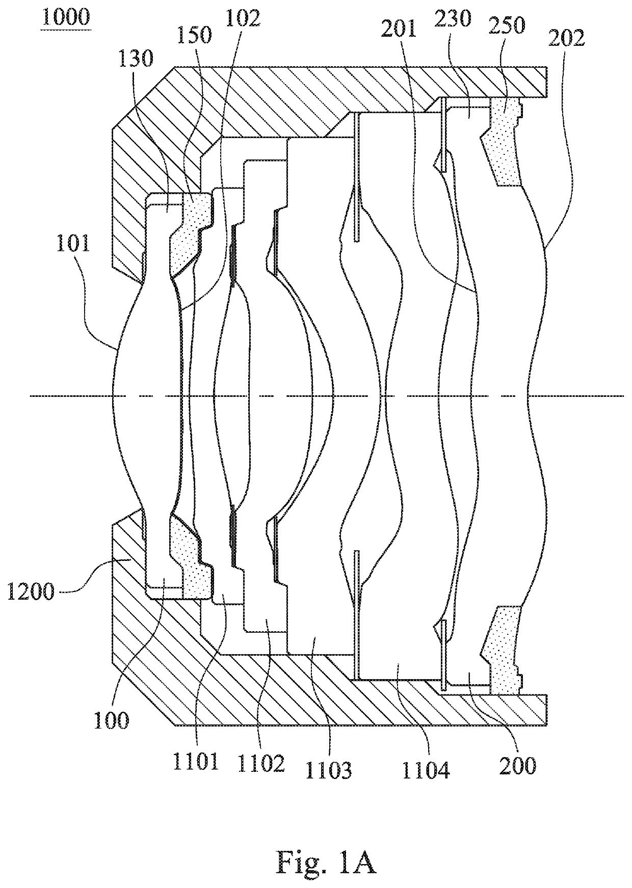
[0031]FIG. 1A is a schematic view of an imaging lens assembly 1000 according to the 1st embodiment of the present disclosure. In FIG. 1A, the imaging lens assembly 1000 includes a plurality of lens elements, wherein two of the lens elements are dual molded lens elements 100 and 200.

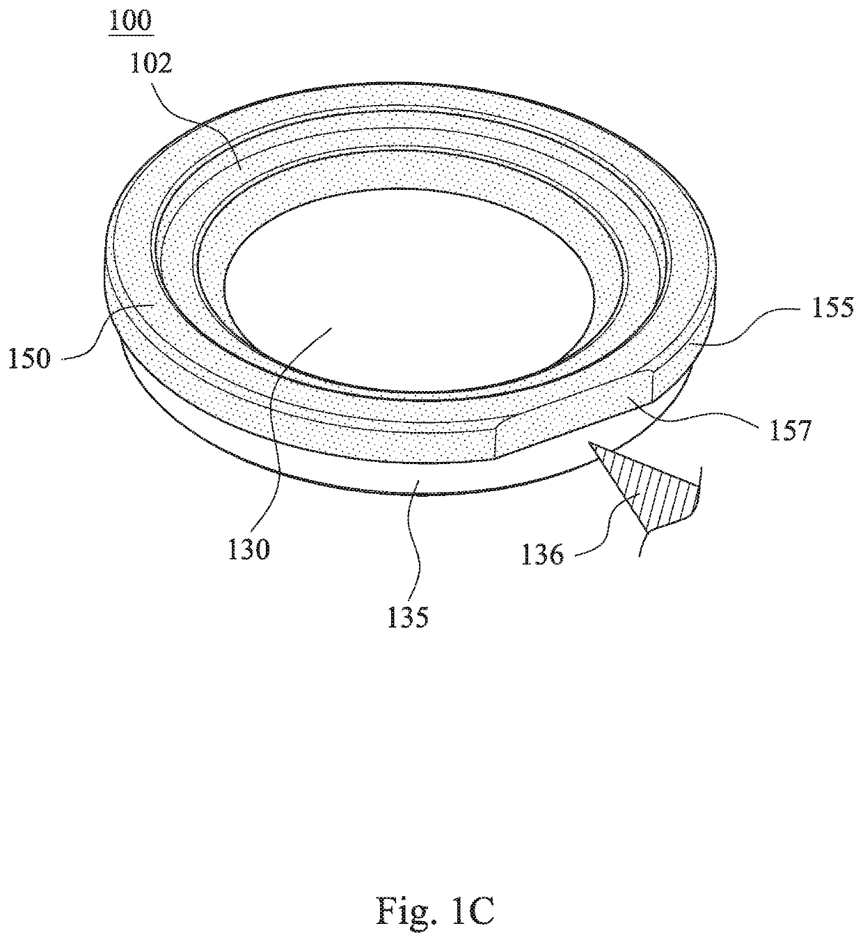
[0032]FIG. 1B is a schematic view of the dual molded lens element 100 according to the 1st embodiment. In FIG. 1A and FIG. 1B, the dual molded lens element 100 includes a light transmitting portion 130 and a light absorbing portion 150, wherein the light transmitting portion 130 and the light absorbing portion 150 of the dual molded lens element 100 are formed by a dual-shot injection molding method or a dual-shot molding method.

[0033]The dual molded lens element 100 has an object-side surface 101, an image-side surface 102 and a lens annular surface 105. The object-side surface 101 is a surface facing an imaged object (not shown herein) of the dual molded lens element 100. The image-side surface 102 is a...

2nd embodiment

[0066]FIG. 2A is a schematic view of an imaging lens assembly 3000 according to the 2nd embodiment of the present disclosure. In FIG. 2A, the imaging lens assembly 3000 includes a plurality of lens elements, wherein one of the lens elements are a dual molded lens element 300.

[0067]FIG. 2B is a schematic view of the dual molded lens element 300 according to the 2nd embodiment. In FIG. 2A and FIG. 2B, the dual molded lens element 300 includes a light transmitting portion 330 and a light absorbing portion 350, wherein the light transmitting portion 330 and the light absorbing portion 350 of the dual molded lens element 300 are formed by a dual-shot injection molding method.

[0068]The dual molded lens element 300 has an object-side surface 301, an image-side surface 302 and a lens annular surface 305. The object-side surface 301 is a surface facing an imaged object (not shown herein) of the dual molded lens element 300. The image-side surface 302 is a surface facing an image surface (not...

3rd embodiment

[0082]FIG. 3 shows an electronic device 10 according to the 3rd embodiment of the present disclosure. The electronic device 10 of the 3rd embodiment is a smart phone, wherein the electronic device 10 includes an imaging lens module 11. The imaging lens module 11 includes an imaging lens assembly (not shown herein) according to the present disclosure. Therefore, it is favorable for improving the image quality so as to satisfy the requirements of high-end electronic devices with camera functionalities. Furthermore, the imaging lens module 11 can further include an image sensor (not shown herein) disposed on or near an image surface (not shown herein) of the imaging lens assembly. Preferably, the electronic device 10 can further include but not limited to a display, a control unit, a storage unit, a random access memory unit (RAM), a read-only memory unit (ROM) or a combination thereof.


PUM

PropertyMeasurementUnit
widthaaaaaaaaaa
widthaaaaaaaaaa
plasticaaaaaaaaaa

Abstract

An imaging lens assembly includes a plurality of lens elements, wherein at least one of the lens elements is a dual molded lens element. The dual molded lens element includes a light transmitting portion and a light absorbing portion. The light transmitting portion includes an effective optical section and a first annular surface. The light absorbing portion is located on at least one surface of an object-side surface and an image-side surface of the dual molded lens element, wherein a plastic material and a color of the light absorbing portion are different from a plastic material and a color of the light transmitting portion, and the light absorbing portion includes an opening and a second annular surface. A step surface of the second annular surface is formed by the first annular surface and the second annular surface.

Description

RELATED APPLICATIONS[0001]This application is a Continuation of application Ser. No. 15 / 201,656, filed Jul. 5, 2016, which claims priority to Taiwan Application Serial Number 105114304, filed May 9, 2016, which is herein incorporated by reference.BACKGROUNDTechnical Field[0002]The present disclosure relates to an imaging lens assembly. More particularly, the present disclosure relates to a compact imaging lens assembly which is applicable to electronic devices.Description of Related Art[0003]Due to the popularity of personal electronic products and mobile communication products having camera functionalities, such as smart phones and tablet personal computers, the demand for compact imaging lens assemblies has been increasing and the requirements for high resolution and image quality of present compact imaging lens assemblies increase significantly.[0004]A plastic lens element is generally used to effectively reduce the manufacturing cost of the imaging lens assembly. A conventional ...

Claims


Application Information

Patent Timeline
Patent Type & Authority Applications(United States)
IPC IPC(8): G02B13/00G02B1/04G02B1/11G02B5/00
CPCG02B5/003G02B13/002G02B13/0055G02B1/11G02B1/041G02B13/18
Inventor CHOU, MING-TALAI, I-WEI
Owner LARGAN PRECISION
Why Eureka
Try Eureka